Wide-Boy64 Research
- Overview
- Wide-Boy64 CGB
- Wide-Boy64 AGB
- Schematics and ideas for building a Wide-Boy64 clone
- Random stuff
- Links
Overview
I got my hands on a Wide-Boy64 AGB that I found on eBay. It's in a very good condition.

Picture 1
Wide-Boy64 AGB
It came with this small cable. I don't know what this is used for.
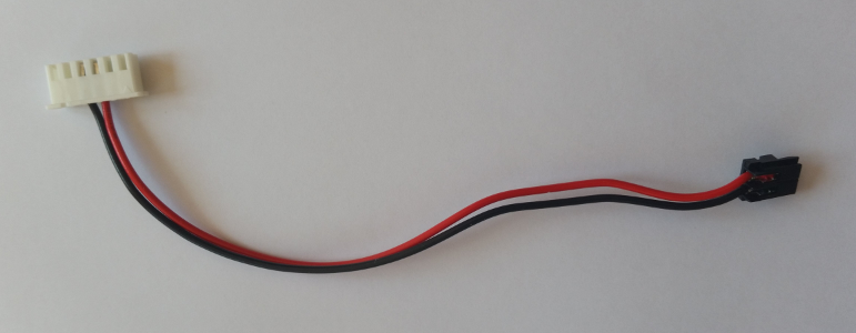
Picture 2
Cable that came with the Wide-Boy64
You can't connect any regular Game Boy to a Wide-Boy. The ones you use as a controller for the Wide-Boy don't have a Game Boy CPU. They have a different PCB that just connects the cartridge port to the display, buttons and the audio amplifier. So they just act as an I/O device.
Wide-Boy64 CGB
Since I don't have the CGB variant of the Wide-Boy64 (yet), I can only describe its adapter here.
CGB Adapter
This is the CGB Adapter I bought:


Picture 3&4
Wide-Boy64 CGB Adapter


Picture 5&6
Wide-Boy64 CGB Adapter PCB
I have drawn a schematic for the PCB: dmg_cart_probe.pdf
I labelled the pins on the cartridge connector with the signals that they usually have on a cartridge (address, data, ...), not the display and button signals that the Wide-Boy puts onto them. The fact that they didn't connect pin 31 (the analog pin) makes me think that this PCB wasn't designed specifically for the Wide-Boy in mind. They might have used this for probing the signals between a Game Boy and a cartridge. (Notice the silk print on the PCB: "DMG CARTRIDGE PROBE") It wouldn't make any sense to not use pin 31 otherwise.
Wide-Boy64 AGB
Components
Here is what I found out about the main components inside the Wide-Boy64 AGB. (Higher resolution pictures can be found in my Game Boy database.)

Picture 7
Components of the Wide-Boy64 AGB
The EEPROM in the bottom left (BU9850) is used in many N64 cartridges that allow to save the game. I don't
know what it is used for in the Wide-Boy. My guess is, they designed it in just in case they need it, but then
never used it for anything. The Wide-Boy64 AGB does not save any settings. It doesn't even have a menu or
something. I haven't checked the contents of this EEPROM yet. I expect it to be all 0xFF. Ah, and yes, it is
connected to the N64 connector at the bottom, so it can be accessed by the N64.
UPDATE: A dump of the EEPROM was done by togemet2:
See GitHub discussion.
(The EEPROM is not empty!)
In the same GitHub discussion, I was informed that the Wide-Boy has a menu that can be accessed when attaching
a second controller to the N64. The information came from this
website. I tried it out and it works. You actually need a
second controller for the menu to work. Both controllers need to be plugged in ports 1 & 2 during boot.
You access the menu by pressing Start on the second controller. Color saturation and brightness of the Game Boy
image can be adjusted in this menu. There is also the software version shown in the bottom right corner. I noticed
that the color and brightness values that you configure in this menu are persistent across power cycles. This
means that those settings are stored in the EEPROM.
There is a second place at the top center of the PCB where a Game Boy External Link Port could be soldered in. Seems like when the PCB was designed, they haven't decided yet where to put the connector.
Luckily, the CIC, EEPROM and PROM chips are socketed. This makes it easy to change the region and dump the EEPROM and PROM contents. The Flash is not socketed though.
The clock generator (U15) to the left of the FPGA provides a ~48.6 MHz clock to the FPGA pin 70. See page 3
of my schematic of the Wide-Boy64 AGB for details: wideboy64agb_sch.pdf
Note that the 250 MHz clock output (RCLK) just gets drained through resistor R24.
Spartan bitstream
I was able to dump the FPGA bitstream from the PROM with an iCE40HX-8K Breakout Board.
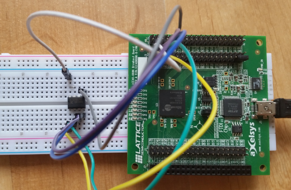
Picture 8
Wide-Boy64 AGB PROM connected to iCE40HX-8K Breakout Board
The code I used for dumping it on a 1Mbit UART can be found here.
The PROM contains 179160 bits (22395 bytes) and when stored LSB-first it has the following hashes:
- MD5: 536e776798fa2ab103e49cd322fb5669
- SHA256: b41f2e84b0d14a2065dfcc17bfb7d49056a277c9c2f0ace1124c7e48b831b49f
I also made an open-source programming device for those PROM chips.
Flash content
I dumped the flash content in two different ways: First by dumping the Wide-Boy like an N64 cartridge, and second by desoldering the flash chip, putting it into a socket and connecting it to an iCE40HX-8K Breakout Board.
For me, the Retrode 2 looked like the best option for dumping N64 cartridges, because it doesn't require any proprietary software that only runs on garbage operating systems that you are even expected to pay money for. It just acts as a USB storage device. The problem with the Retrode 2 however is, that it isn't actually designed for dumping development cartridges like the Wide-Boy. It doesn't provide the 12 volts that the Wide-Boy requires. But if you solder some wires at the back of the regulators U3 or U4, which take the 12 V as inputs, you can just power them externally.
The flash when dumped as a 4 MiB N64 cartridge has the following hashes:
- MD5: 035d3b6fea083ab2d779c0f611ef11fa
- SHA256: 06da122ff65557ecc4c258a1338854cfcaafbadc04c432e5e1c183e34f411209
I used this socket connected to an iCE40HX-8K Breakout Board for dumping the desoldered flash chip directly.

Picture 9
Wide-Boy64 AGB Flash connected to iCE40HX-8K Breakout Board
The code I used for dumping it on a 1Mbit UART can be found here.
The flash is 4 MiB in size. The first half of the flash turned out to be empty (0xFF). At address 0x200000 the actual data starts that I had also seen after the N64 cartridge dump. But the data is byte swapped in 16 bit words. Here's how the hex dumps look like:
Dumped as cartridge:
00000000  80 37 12 40 00 00 00 0f  80 02 5c 00 00 00 14 49  |.7.@......\....I|
00000010  d1 71 2d 97 9f 82 40 91  00 00 00 00 00 00 00 00  |.q-...@.........|
00000020  00 00 00 00 00 00 00 00  00 00 00 00 00 00 00 00  |................|
*
00000040  40 80 68 00 40 80 48 00  40 80 58 00 3c 08 a4 70  |@.h.@.H.@.X.<..p|
...
Dumped directly:
00000000  ff ff ff ff ff ff ff ff  ff ff ff ff ff ff ff ff  |................|
*
00200000  37 80 40 12 00 00 0f 00  02 80 00 5c 00 00 49 14  |7.@........\..I.|
00200010  71 d1 97 2d 82 9f 91 40  00 00 00 00 00 00 00 00  |q..-...@........|
00200020  00 00 00 00 00 00 00 00  00 00 00 00 00 00 00 00  |................|
*
00200040  80 40 00 68 80 40 00 48  80 40 00 58 08 3c 70 a4  |.@.h.@.H.@.X.<p.|
...
The flash when dumped directly has the following hashes:
- MD5: 529f0a6d80ef479b68c9c18e6d225b7f
- SHA256: 3391da27efea6931ffe35a09d844dcff794e29a07d9c01a3b329469acf312d36
I also executed the "Read Identifier Codes" command on the flash (see datasheet) and read the entire thing again. I didn't find anything. Only the factory part of the OTP block is programmed. The customer part is 0xFF.
40-pin connector (CN3) pinout on Wide-Boy64 AGB
| Pin# | Usage | To CPU | To FPGA | Pin# | Usage | To CPU | To FPGA | ||||
|---|---|---|---|---|---|---|---|---|---|---|---|
| 1 | Audio R | 6 | SO1 | - | 21 | LCD Data B2 | 100 | LDB2 | 86 | I/O | |
| 2 | Audio L | 7 | SO2 | - | 22 | LCD Data B3 | 99 | LDB3 | 87 | I/O | |
| 3 | Button B | 5 | P1 | 61 | I/O | 23 | LCD Data B4 | 98 | LDB4 | 88 | I/O (D4) |
| 4 | Button A | 4 | P0 | 62 | I/O | 24 | LCD Data B5 | 97 | LDB5 | 89 | I/O |
| 5 | Button R | 3 | P8 | 63 | I/O | 25 | LCD Data G1 | 96 | LDG1 | 92 | I/O (D3) |
| 6 | Button Start | 127 | P3 | 65 | I/O | 26 | LCD Data G2 | 95 | LDG2 | 93 | I/O |
| 7 | Button Select | 126 | P2 | 66 | I/O | 27 | LCD Data G3 | 94 | LDG3 | 94 | I/O |
| 8 | Button D-Right | 123 | P4 | 67 | I/O | 28 | GND | 102,128,... | GND | 81,91,... | GND |
| 9 | Button D-Down | 122 | P7 | 68 | I/O | 29 | LCD Data G4 | 93 | LDG4 | 95 | I/O |
| 10 | Button D-Left | 121 | P5 | 69 | I/O | 30 | LCD Data G5 | 92 | LDG5 | 96 | I/O (D2) |
| 11 | Button D-Up | 120 | P6 | 75 | I/O (D7) | 31 | LCD Data R1 | 91 | LDR1 | 97 | I/O |
| 12 | Button L | 119 | P9 | 77 | I/O | 32 | LCD Data R2 | 90 | LDR2 | 98 | I/O |
| 13 | LCD VSHD Enable? | 118 | R10 | 78 | I/O | 33 | LCD Data R3 | 89 | LDR3 | 99 | I/O |
| 14 | AGB-REG Switch? | 108 | REVC | 79 | I/O (D6) | 34 | LCD Data R4 | 88 | LDR4 | 101 | I/O (D1) |
| 15 | LCD Mode? | 107 | MOD | 80 | I/O | 35 | LCD Data R5 | 87 | LDR5 | 102 | I/O |
| 16 | LCD SPS? | 106 | SPS | 82 | I/O | 36 | GND | 102,128,... | GND | 81,91,... | GND |
| 17 | LCD CLS? | 105 | CLS | 83 | I/O | 37 | LCD PS? | 86 | PS | 103 | I/O |
| 18 | LCD SPL? | 104 | SPL | 84 | I/O (D5) | 38 | LCD LP? | 85 | LP | 104 | I/O |
| 19 | GND | 102,128,... | GND | 81,91,... | GND | 39 | LCD Data Clock? | 84 | DCK | 112 | I/O, GCK7 |
| 20 | LCD Data B1 | 101 | LDB1 | 85 | I/O | 40 | 3.3 V Supply | 1,103 | VDD3 | 128,144,... | VCC |
Table 1
Connections from Wide-Boy64 AGB 40-pin connector (CN3) to AGB CPU and Spartan FPGA
Memories connected to FPGA (and each other) on Wide-Boy64 AGB
Flash
| Pin# | Name | To FPGA | To DRAM | Pin# | Name | To FPGA | To DRAM | ||||
|---|---|---|---|---|---|---|---|---|---|---|---|
| 1 | A15 | 21 | I/O | - | 25 | A0 | 3 | I/O | 23 | A0 | |
| 2 | A14 | 20 | I/O | 21 | BA1(A12) | 26 | CE# | 28 | I/O | - | |
| 3 | A13 | 19 | I/O | 20 | BA0(A13) | 27 | GND | 27,... | GND | 41,46,... | VSS,VSSQ |
| 4 | A12 | 16 | I/O | 36 | NC | 28 | OE# | 29 | I/O | 17 | !CAS |
| 5 | A11 | 15 | I/O | 35 | A11 | 29 | DQ0 | 47 | I/O | 2 | DQ0 |
| 6 | A10 | 14 | I/O | 22 | A10 | 30 | DQ8 | 58 | I/O | 42 | DQ8 |
| 7 | A9 | 13 | I/O | 34 | A9 | 31 | DQ1 | 46 | I/O | 4 | DQ1 |
| 8 | A8 | 12 | I/O | 33 | A8 | 32 | DQ9 | 57 | I/O | 44 | DQ9 |
| 9 | A19 | 25 | I/O | - | 33 | DQ2 | 43 | I/O | 5 | DQ2 | |
| 10 | A20 | 26 | I/O | - | 34 | DQ10 | 56 | I/O | 45 | DQ10 | |
| 11 | WE# | 30 | I/O | 16 | !WE | 35 | DQ3 | 42 | I/O | 7 | DQ3 |
| 12 | RP# | 72 | DONE | - | 36 | DQ11 | 52 | I/O | 47 | DQ11 | |
| 13 | VCCW | 144,... | VCC | 1,3,... | VCC,VCCQ | 37 | VCC | 144,... | VCC | 1,3,... | VCC,VCCQ |
| 14 | WP# | 144,... | VCC | 1,3,... | VCC,VCCQ | 38 | DQ4 | 41 | I/O | 8 | DQ4 |
| 15 | RY/BY# | - | - | 39 | DQ12 | 51 | I/O | 48 | DQ12 | ||
| 16 | A18 | 24 | I/O | - | 40 | DQ5 | 39 | I/O, GCK3 | 10 | DQ5 | |
| 17 | A17 | 23 | I/O | - | 41 | DQ13 | 50 | I/O | 50 | DQ13 | |
| 18 | A7 | 11 | I/O, TMS | 32 | A7 | 42 | DQ6 | 33 | I/O, GCK2 | 11 | DQ6 |
| 19 | A6 | 10 | I/O | 31 | A6 | 43 | DQ14 | 49 | I/O | 51 | DQ14 |
| 20 | A5 | 9 | I/O | 30 | A5 | 44 | DQ7 | 32 | I/O | 13 | DQ7 |
| 21 | A4 | 7 | I/O, TCK | 29 | A4 | 45 | DQ15/A-1 | 48 | I/O | 53 | DQ15 |
| 22 | A3 | 6 | I/O, TDI | 26 | A3 | 46 | GND | 27,... | GND | 41,46,... | VSS,VSSQ |
| 23 | A2 | 5 | I/O | 25 | A2 | 47 | BYTE# | 144,... | VCC | 1,3,... | VCC,VCCQ |
| 24 | A1 | 4 | I/O | 24 | A1 | 48 | A16 | 22 | I/O | - | |
Table 2
Connections from Flash on Wide-Boy64 AGB to Spartan FPGA and DRAM
DRAM
| Pin# | Name | To FPGA | To Flash | Pin# | Name | To FPGA | To Flash | ||||
|---|---|---|---|---|---|---|---|---|---|---|---|
| 1 | VCC | 144,... | VCC | 37,13,... | VCC,VCCW | 28 | VSS | 27,... | GND | 27,... | GND |
| 2 | DQ0 | 47 | I/O | 29 | DQ0 | 29 | A4 | 7 | I/O, TCK | 21 | A4 |
| 3 | VCCQ | 144,... | VCC | 37,13,... | VCC,VCCW | 30 | A5 | 9 | I/O | 20 | A5 |
| 4 | DQ1 | 46 | I/O | 31 | DQ1 | 31 | A6 | 10 | I/O | 19 | A6 |
| 5 | DQ2 | 43 | I/O | 33 | DQ2 | 32 | A7 | 11 | I/O, TMS | 18 | A7 |
| 6 | VSSQ | 27,... | GND | 27,... | GND | 33 | A8 | 12 | I/O | 8 | A8 |
| 7 | DQ3 | 42 | I/O | 35 | DQ3 | 34 | A9 | 13 | I/O | 7 | A9 |
| 8 | DQ4 | 41 | I/O | 38 | DQ4 | 35 | A11 | 15 | I/O | 5 | A11 |
| 9 | VCCQ | 144,... | VCC | 37,13,... | VCC,VCCW | 36 | NC | 16 | I/O | 4 | A12 |
| 10 | DQ5 | 39 | I/O, GCK3 | 40 | DQ5 | 37 | CKE | 144,... | VCC | 37,13,... | VCC,VCCW |
| 11 | DQ6 | 33 | I/O, GCK2 | 42 | DQ6 | 38 | CLK | 106 | I/O, GCK6 (DOUT) | - | |
| 12 | VSSQ | 27,... | GND | 27,... | GND | 39 | UDQM | 113 | I/O | - | |
| 13 | DQ7 | 32 | I/O | 44 | DQ7 | 40 | NC | - | - | ||
| 14 | VCC | 144,... | VCC | 37,13,... | VCC,VCCW | 41 | VSS | 27,... | GND | 27,... | GND |
| 15 | LDQM | 115 | I/O (CS1) | - | 42 | DQ8 | 58 | I/O | 30 | DQ8 | |
| 16 | !WE | 30 | I/O | 11 | WE# | 43 | VCCQ | 144,... | VCC | 37,13,... | VCC,VCCW |
| 17 | !CAS | 29 | I/O | 28 | OE# | 44 | DQ9 | 57 | I/O | 32 | DQ9 |
| 18 | !RAS | 111 | I/O | - | 45 | DQ10 | 56 | I/O | 34 | DQ10 | |
| 19 | !CS | 31 | I/O | - | 46 | VSSQ | 27,... | GND | 27,... | GND | |
| 20 | BA0(A13) | 19 | I/O | 3 | A13 | 47 | DQ11 | 52 | I/O | 36 | DQ11 |
| 21 | BA1(A12) | 20 | I/O | 2 | A14 | 48 | DQ12 | 51 | I/O | 39 | DQ12 |
| 22 | A10 | 14 | I/O | 6 | A10 | 49 | VCCQ | 144,... | VCC | 37,13,... | VCC,VCCW |
| 23 | A0 | 3 | I/O | 25 | A0 | 50 | DQ13 | 50 | I/O | 41 | DQ13 |
| 24 | A1 | 4 | I/O | 24 | A1 | 51 | DQ14 | 49 | I/O | 43 | DQ14 |
| 25 | A2 | 5 | I/O | 23 | A2 | 52 | VSSQ | 27,... | GND | 27,... | GND |
| 26 | A3 | 6 | I/O, TDI | 22 | A3 | 53 | DQ15 | 48 | I/O | 45 | DQ15/A-1 |
| 27 | VCC | 144,... | VCC | 37,13,... | VCC,VCCW | 54 | VSS | 27,... | GND | 27,... | GND |
Table 3
Connections from DRAM on Wide-Boy64 AGB to Spartan FPGA and Flash
Voltages measured on regulators on Wide-Boy64 AGB
| Pin# | Name | U3 | U4 | U5 |
|---|---|---|---|---|
| 1 | VIN | 11.5 V | 11.5 V | 5 V |
| 2 | VO | 2.5 V | 5 V | 3.3 V |
| 3 | GND | 0 V | 0 V | 0 V |
| 4 | VADJ/VC | 1.25 V | 2.5 V | 1.25 V |
Table 4
Voltages measured at the three voltage regulators at the bottom of the Wide-Boy64 AGB PCB
N64 cartridge connector on Wide-Boy64 AGB
| Pin# | Name | To CN2 | To component pin# | Pin# | Name | To CN2 | To component pin# | ||||
|---|---|---|---|---|---|---|---|---|---|---|---|
| 1 | GND | 1,2,9,10,37,38 | GND | 26 | GND | 1,2,9,10,37,38 | GND | ||||
| 2 | GND | 1,2,9,10,37,38 | GND | 27 | GND | 1,2,9,10,37,38 | GND | ||||
| 3 | AD15 | 3 | FPGA | 139 | I/O | 28 | AD0 | 4 | FPGA | 140 | I/O |
| 4 | AD14 | 5 | FPGA | 136 | I/O | 29 | AD1 | 6 | FPGA | 138 | I/O |
| 5 | AD13 | 7 | FPGA | 134 | I/O | 30 | AD2 | 8 | FPGA | 135 | I/O |
| 6 | GND | 1,2,9,10,37,38 | GND | 31 | GND | 1,2,9,10,37,38 | GND | ||||
| 7 | AD12 | 11 | FPGA | 132 | I/O | 32 | AD3 | 12 | FPGA | 133 | I/O |
| 8 | !WRITE | 13 | FPGA | 2 | I/O, GCK1 | 33 | ALE_L | 14 | FPGA | 143 | I/O, GCK8 |
| 9 | VCC* | 15,16 | EEPROM;CIC;U6 | 8;1,16;5 | VCC | 34 | VCC* | 15,16 | EEPROM;CIC;U6 | 8;1,16;5 | VCC |
| 10 | !READ | 17 | FPGA | 142 | I/O | 35 | ALE_H | 18 | FPGA | 141 | I/O |
| 11 | AD11 | 19 | FPGA | 130 | I/O | 36 | AD4 | 20 | FPGA | 131 | I/O |
| 12 | AD10 | 21 | FPGA | 126 | I/O | 37 | AD5 | 22 | FPGA | 129 | I/O |
| 13 | 12V | 23,24 | Regs U3;U4 | 1 | VIN | 38 | 12V | 23,24 | Regs U3;U4 | 1 | VIN |
| 14 | NC | - | - | 39 | NC | - | - | ||||
| 15 | AD9 | 25 | FPGA | 124 | I/O | 40 | AD6 | 26 | FPGA | 125 | I/O |
| 16 | AD8 | 27 | FPGA | 122 | I/O | 41 | AD7 | 28 | FPGA | 123 | I/O |
| 17 | VCC* | 15,16 | EEPROM;CIC;U6 | 8;1,16;5 | VCC | 42 | VCC* | 15,16 | EEPROM;CIC;U6 | 8;1,16;5 | VCC |
| 18 | CIC_DIO | 29 | CIC | 15 | DIO | 43 | CIC_DCLK | 30 | CIC | 14 | DCLK |
| 19 | 1.6MHZ | 31 | EEPROM;CIC | 3;11 | CLK_IN | 44 | JTAG_CLK_R4300 | 32 | FPGA | 120 | I/O |
| 20 | !COLD_RESET | 33 | FPGA;EEPROM;CIC | 121;6;9 | I/O;!RST | 45 | !NMI_R4300 | 34 | FPGA | 119 | I/O |
| 21 | S_DAT | 35 | EEPROM | 5 | DATA | 46 | VIDEO_CLK | 36 | FPGA | 117 | I/O |
| 22 | GND | 1,2,9,10,37,38 | GND | 47 | GND | 1,2,9,10,37,38 | GND | ||||
| 23 | GND | 1,2,9,10,37,38 | GND | 48 | GND | 1,2,9,10,37,38 | GND | ||||
| 24 | LAUDIO | 39 | Cap C6 | 49 | RAUDIO | 40 | Cap C7 | ||||
| 25 | GND | 1,2,9,10,37,38 | GND | 50 | GND | 1,2,9,10,37,38 | GND | ||||
Table 5
Connections from N64 cartridge connector on Wide-Boy64 AGB to CN2 and other components.
* VCC on the N64 cartridge connector is 3.3 V, but it is not connected to the VCC of the FPGA or the AGB CPU.
It only powers the CIC, EEPROM and Reset Controller (U6).
FPGA pin connections on Wide-Boy64 AGB
| Pin# | Name | Usage | To component pin# | To component pin# | To component pin# | ||||||
|---|---|---|---|---|---|---|---|---|---|---|---|
| 1 | GND | ||||||||||
| 2 | I/O, GCK1 | N64 !WRITE | N64 connector | 8 | !WRITE | - | - | ||||
| 3 | I/O | Flash/DRAM A0 | Flash | 25 | A0 | DRAM | 23 | A0 | - | ||
| 4 | I/O | Flash/DRAM A1 | Flash | 24 | A1 | DRAM | 24 | A1 | - | ||
| 5 | I/O | Flash/DRAM A2 | Flash | 23 | A2 | DRAM | 25 | A2 | - | ||
| 6 | I/O, TDI | Flash/DRAM A3 | Flash | 22 | A3 | DRAM | 26 | A3 | - | ||
| 7 | I/O, TCK | Flash/DRAM A4 | Flash | 21 | A4 | DRAM | 29 | A4 | - | ||
| 8 | GND | ||||||||||
| 9 | I/O | Flash/DRAM A5 | Flash | 20 | A5 | DRAM | 30 | A5 | - | ||
| 10 | I/O | Flash/DRAM A6 | Flash | 19 | A6 | DRAM | 31 | A6 | - | ||
| 11 | I/O, TMS | Flash/DRAM A7 | Flash | 18 | A7 | DRAM | 32 | A7 | - | ||
| 12 | I/O | Flash/DRAM A8 | Flash | 8 | A8 | DRAM | 33 | A8 | - | ||
| 13 | I/O | Flash/DRAM A9 | Flash | 7 | A9 | DRAM | 34 | A9 | - | ||
| 14 | I/O | Flash/DRAM A10 | Flash | 6 | A10 | DRAM | 22 | A10 | - | ||
| 15 | I/O | Flash/DRAM A11 | Flash | 5 | A11 | DRAM | 35 | A11 | - | ||
| 16 | I/O | Flash A12 | Flash | 4 | A12 | DRAM | 36 | NC | - | ||
| 17 | GND | ||||||||||
| 18 | VCC | ||||||||||
| 19 | I/O | Flash/DRAM A13 | Flash | 3 | A13 | DRAM | 20 | BA0(A13) | - | ||
| 20 | I/O | Flash A14; DRAM A12 | Flash | 2 | A14 | DRAM | 21 | BA1(A12) | - | ||
| 21 | I/O | Flash A15 | Flash | 1 | A15 | - | - | ||||
| 22 | I/O | Flash A16 | Flash | 48 | A16 | - | - | ||||
| 23 | I/O | Flash A17 | Flash | 17 | A17 | - | - | ||||
| 24 | I/O | Flash A18 | Flash | 16 | A18 | - | - | ||||
| 25 | I/O | Flash A19 | Flash | 9 | A19 | - | - | ||||
| 26 | I/O | Flash A20 | Flash | 10 | A20 | - | - | ||||
| 27 | GND | ||||||||||
| 28 | I/O | Flash !CE | Flash | 26 | CE# | - | - | ||||
| 29 | I/O | Flash !OE; DRAM !CAS | Flash | 28 | OE# | DRAM | 17 | !CAS | - | ||
| 30 | I/O | Flash/DRAM !WE | Flash | 11 | WE# | DRAM | 16 | !WE | - | ||
| 31 | I/O | DRAM !CS | - | DRAM | 19 | !CS | - | ||||
| 32 | I/O | Flash/DRAM DQ7 | Flash | 44 | DQ7 | DRAM | 13 | DQ7 | - | ||
| 33 | I/O, GCK2 | Flash/DRAM DQ6 | Flash | 42 | DQ6 | DRAM | 11 | DQ6 | - | ||
| 34 | M1 | Cfg. Mode (NC; M1=high) | - | - | - | ||||||
| 35 | GND | ||||||||||
| 36 | M0 | Cfg. Mode (M0=low) | GND | - | - | ||||||
| 37 | VCC | ||||||||||
| 38 | !PWRDWN | (Never Power Down) | VCC | - | - | ||||||
| 39 | I/O, GCK3 | Flash/DRAM DQ5 | Flash | 40 | DQ5 | DRAM | 10 | DQ5 | - | ||
| 40 | I/O (HDC) | ? | - | - | Testpoint CP1 | ||||||
| 41 | I/O | Flash/DRAM DQ4 | Flash | 38 | DQ4 | DRAM | 8 | DQ4 | - | ||
| 42 | I/O | Flash/DRAM DQ3 | Flash | 35 | DQ3 | DRAM | 7 | DQ3 | - | ||
| 43 | I/O | Flash/DRAM DQ2 | Flash | 33 | DQ2 | DRAM | 5 | DQ2 | - | ||
| 44 | I/O (!LDC) | PROM !CE | PROM | 4 | !CE | - | - | ||||
| 45 | GND | ||||||||||
| 46 | I/O | Flash/DRAM DQ1 | Flash | 31 | DQ1 | DRAM | 4 | DQ1 | - | ||
| 47 | I/O | Flash/DRAM DQ0 | Flash | 29 | DQ0 | DRAM | 2 | DQ0 | - | ||
| 48 | I/O | Flash/DRAM DQ15 | Flash | 45 | DQ15/A-1 | DRAM | 53 | DQ15 | - | ||
| 49 | I/O | Flash/DRAM DQ14 | Flash | 43 | DQ14 | DRAM | 51 | DQ14 | - | ||
| 50 | I/O | Flash/DRAM DQ13 | Flash | 41 | DQ13 | DRAM | 50 | DQ13 | - | ||
| 51 | I/O | Flash/DRAM DQ12 | Flash | 39 | DQ12 | DRAM | 48 | DQ12 | - | ||
| 52 | I/O | Flash/DRAM DQ11 | Flash | 36 | DQ11 | DRAM | 47 | DQ11 | - | ||
| 53 | I/O (!INIT) | PROM OE | PROM | 3 | OE/!RESET | - | - | ||||
| 54 | VCC | ||||||||||
| 55 | GND | ||||||||||
| 56 | I/O | Flash/DRAM DQ10 | Flash | 34 | DQ10 | DRAM | 45 | DQ10 | - | ||
| 57 | I/O | Flash/DRAM DQ9 | Flash | 32 | DQ9 | DRAM | 44 | DQ9 | - | ||
| 58 | I/O | Flash/DRAM DQ8 | Flash | 30 | DQ8 | DRAM | 42 | DQ8 | - | ||
| 59 | I/O | AGB-AMP !Standby? | AGB-AMP | 12 | !STB | - | - | ||||
| 60 | I/O | ? | - | - | Testpoint CP2 | ||||||
| 61 | I/O | Button B | CPU | 5 | P1 | CN3 | 3 | - | |||
| 62 | I/O | Button A | CPU | 4 | P0 | CN3 | 4 | - | |||
| 63 | I/O | Button R | CPU | 3 | P8 | CN3 | 5 | - | |||
| 64 | GND | ||||||||||
| 65 | I/O | Button Start | CPU | 127 | P3 | CN3 | 6 | - | |||
| 66 | I/O | Button Select | CPU | 126 | P2 | CN3 | 7 | - | |||
| 67 | I/O | Button D-Right | CPU | 123 | P4 | CN3 | 8 | - | |||
| 68 | I/O | Button D-Down | CPU | 122 | P7 | CN3 | 9 | - | |||
| 69 | I/O | Button D-Left | CPU | 121 | P5 | CN3 | 10 | - | |||
| 70 | I/O, GCK4 | 48.681812 MHz | MX8350 (U15) | 3 | VCLK | - | - | ||||
| 71 | GND | ||||||||||
| 72 | DONE | Flash !RESET | Flash | 12 | RP# | - | Testpoint CP5 | ||||
| 73 | VCC | ||||||||||
| 74 | !PROGRAM | 48.681812 MHz Enable | MX8350 (U15) | 14 | !RESET | - | - | ||||
| 75 | I/O (D7) | Button D-Up | CPU | 120 | P6 | CN3 | 11 | - | |||
| 76 | I/O, GCK5 | ? | - | - | Testpoint CP3 | ||||||
| 77 | I/O | Button L | CPU | 119 | P9 | CN3 | 12 | - | |||
| 78 | I/O | LCD VSHD Enable? | CPU | 118 | R10 | CN3 | 13 | - | |||
| 79 | I/O (D6) | AGB-REG Switch? | CPU | 108 | REVC | CN3 | 14 | - | |||
| 80 | I/O | LCD Mode? | CPU | 107 | MOD | CN3 | 15 | - | |||
| 81 | GND | ||||||||||
| 82 | I/O | LCD SPS? | CPU | 106 | SPS | CN3 | 16 | - | |||
| 83 | I/O | LCD CLS? | CPU | 105 | CLS | CN3 | 17 | - | |||
| 84 | I/O (D5) | LCD SPL? | CPU | 104 | SPL | CN3 | 18 | - | |||
| 85 | I/O | LCD Data B1 | CPU | 101 | LDB1 | CN3 | 20 | - | |||
| 86 | I/O | LCD Data B2 | CPU | 100 | LDB2 | CN3 | 21 | - | |||
| 87 | I/O | LCD Data B3 | CPU | 99 | LDB3 | CN3 | 22 | - | |||
| 88 | I/O (D4) | LCD Data B4 | CPU | 98 | LDB4 | CN3 | 23 | - | |||
| 89 | I/O | LCD Data B5 | CPU | 97 | LDB5 | CN3 | 24 | - | |||
| 90 | VCC | ||||||||||
| 91 | GND | ||||||||||
| 92 | I/O (D3) | LCD Data G1 | CPU | 96 | LDG1 | CN3 | 25 | - | |||
| 93 | I/O | LCD Data G2 | CPU | 95 | LDG2 | CN3 | 26 | - | |||
| 94 | I/O | LCD Data G3 | CPU | 94 | LDG3 | CN3 | 27 | - | |||
| 95 | I/O | LCD Data G4 | CPU | 93 | LDG4 | CN3 | 29 | - | |||
| 96 | I/O (D2) | LCD Data G5 | CPU | 92 | LDG5 | CN3 | 30 | - | |||
| 97 | I/O | LCD Data R1 | CPU | 91 | LDR1 | CN3 | 31 | - | |||
| 98 | I/O | LCD Data R2 | CPU | 90 | LDR2 | CN3 | 32 | - | |||
| 99 | I/O | LCD Data R3 | CPU | 89 | LDR3 | CN3 | 33 | - | |||
| 100 | GND | ||||||||||
| 101 | I/O (D1) | LCD Data R4 | CPU | 88 | LDR4 | CN3 | 34 | - | |||
| 102 | I/O | LCD Data R5 | CPU | 87 | LDR5 | CN3 | 35 | - | |||
| 103 | I/O | LCD PS? | CPU | 86 | PS | CN3 | 37 | - | |||
| 104 | I/O | LCD LP? | CPU | 85 | LP | CN3 | 38 | - | |||
| 105 | I/O (D0, DIN) | PROM DATA | PROM | 1 | DATA | - | - | ||||
| 106 | I/O, GCK6 (DOUT) | DRAM CLK | - | DRAM | 38 | CLK | - | ||||
| 107 | CCLK | PROM CLK | PROM | 2 | CLK | - | - | ||||
| 108 | VCC | ||||||||||
| 109 | O, TDO | ? | - | - | Testpoint CP4 | ||||||
| 110 | GND | ||||||||||
| 111 | I/O | DRAM !RAS | - | DRAM | 18 | !RAS | - | ||||
| 112 | I/O, GCK7 | LCD Data Clock? | CPU | 84 | DCK | CN3 | 39 | - | |||
| 113 | I/O | DRAM UDQM | - | DRAM | 39 | UDQM | - | ||||
| 114 | I/O | CPU !RESET | D4 | K | R6 | - | |||||
| 115 | I/O (CS1) | DRAM LDQM | - | DRAM | 15 | LDQM | - | ||||
| 116 | I/O | Voltage stable? | U6 | 4 | VOUT | - | - | ||||
| 117 | I/O | N64 VIDEO_CLK | N64 connector | 46 | VIDEO_CLK | - | - | ||||
| 118 | GND | ||||||||||
| 119 | I/O | N64 !NMI_R4300 | N64 connector | 45 | !NMI_R4300 | - | - | ||||
| 120 | I/O | N64 JTAG_CLK_R4300 | N64 connector | 44 | !JTAG_CLK_R4300 | - | - | ||||
| 121 | I/O | N64 !COLD_RESET | N64 connector | 20 | !COLD_RESET | EEPROM | 6 | !RST | CIC | 9 | !RST |
| 122 | I/O | N64 AD8 | N64 connector | 16 | AD8 | - | - | ||||
| 123 | I/O | N64 AD7 | N64 connector | 41 | AD7 | - | - | ||||
| 124 | I/O | N64 AD9 | N64 connector | 15 | AD9 | - | - | ||||
| 125 | I/O | N64 AD6 | N64 connector | 40 | AD6 | - | - | ||||
| 126 | I/O | N64 AD10 | N64 connector | 12 | AD10 | - | - | ||||
| 127 | GND | ||||||||||
| 128 | VCC | ||||||||||
| 129 | I/O | N64 AD5 | N64 connector | 37 | AD5 | - | - | ||||
| 130 | I/O | N64 AD11 | N64 connector | 11 | AD11 | - | - | ||||
| 131 | I/O | N64 AD4 | N64 connector | 36 | AD4 | - | - | ||||
| 132 | I/O | N64 AD12 | N64 connector | 7 | AD12 | - | - | ||||
| 133 | I/O | N64 AD3 | N64 connector | 32 | AD3 | - | - | ||||
| 134 | I/O | N64 AD13 | N64 connector | 5 | AD13 | - | - | ||||
| 135 | I/O | N64 AD2 | N64 connector | 30 | AD2 | - | - | ||||
| 136 | I/O | N64 AD14 | N64 connector | 4 | AD14 | - | - | ||||
| 137 | GND | ||||||||||
| 138 | I/O | N64 AD1 | N64 connector | 29 | AD1 | - | - | ||||
| 139 | I/O | N64 AD15 | N64 connector | 3 | AD15 | - | - | ||||
| 140 | I/O | N64 AD0 | N64 connector | 28 | AD0 | - | - | ||||
| 141 | I/O | N64 ALE_H | N64 connector | 35 | ALE_H | - | - | ||||
| 142 | I/O | N64 !READ | N64 connector | 10 | !READ | - | - | ||||
| 143 | I/O, GCK8 | N64 ALE_L | N64 connector | 33 | ALE_L | - | - | ||||
| 144 | VCC | ||||||||||
Table 6
Connections from Spartan FPGA on Wide-Boy64 AGB to other components
Schematics and ideas for building a Wide-Boy64 clone
I finished drawing the schematic of the Wide-Boy64 AGB. For the parts I don't know the exact values yet, I marked them with a question mark (?). Some values I took from the Portuguese Game Boy Advance Service Manual where I thought they are most likely the same parts, but I still put a question mark after the value to emphasize that I'm not 100% sure about them.
Desoldering the Cartridge Slot from a GBA could be a bit of a pain, I haven't tried it yet. I bought them on AliExpress, but those don't have room for that switch, unfortunately.
The Spartan XCS20XL is not produced anymore, but you can still buy some on, again, AliExpress. I wasn't able to find those bitstream PROMs, though. If I'm not able to find one that behaves in a compatible way, then I would use a second FPGA to emulate the behavior of the XC17S20XL PROM. This FPGA could also emulate the N64 CIC. Then it wouldn't be necessary to sacrifice a cartridge for that.
UPDATE: I found the PROM here.
I ordered ten chips, they arrived within five days! I dumped all ten chips to confirm that they are indeed
empty/unused. When dumping those unprogrammed chips, the OE/RESET pin needs to be inverted, because that's
how they are initially, when they are not configured yet.

A better approach would be to replace the outdated Spartan FPGA, but then this would mean one has to implement the decoding of the display signals. The frame buffer interface to the N64 would also have to be replicated. I don't know what is easier: Reverse engineering the interface between the Spartan and the N64 software inside the flash, or writing the N64 code from scratch as well.
Random stuff
Fun fact: On the Wide-Boy64 AGB PCB, the CIC chip is labelled "CTC".

Picture 10
Silk print on the Wide-Boy64 AGB PCB under the CIC and EEPROM chips
I assume the correct notation of Wide-Boy64 is with a hyphen between the words and without a space before the number, like it is printed on the labels on the front and back side of the device. However, on the PCB it is written as one word, WIDEBOY AGB. On Wikipedia and many other sites, it is written as Wide-Boy 64, with a space before the number. TBH, I just mention the different notations here to make this page more likely to show up on Google.
I don't understand for what reason there is a 4.0 V reset controller (U6) on the Wide-Boy64 AGB, watching the 3.3 V coming from the N64. On top of that, they didn't put a capacitor between GND and the VOUT pin, like it is recommended in the data sheet of the PST9140N. They put one between GND and VCC. They also didn't leave the NC pin unconnected; they connected it to GND.
I also took a picture from underneath the flash, while I was dumping it. Maybe it is useful sometime for recreating the PCB:

Picture 11
Wide-Boy64 AGB PCB under the flash chip
Links
- Spartan and Spartan-XL FPGA Families Data Sheet
- Spartan/XL Family One-Time Programmable Configuration PROMs (XC17S00/XL)
- Xilinx Programmer Qualification Specification
- Game Boy Advance service manual and schematics
- µPD45128163 - 128M-bit Synchronous DRAM
- LH28F320BJE-PTTL90 - Flash Memory 32M
- MX8350 - 2 in 1 Rambus Clock Generator
- PQ30RV21 - Variable Output Low Power-Loss Voltage Regulators
- PQ05RF21 - 2A Output, Low Power-Loss Voltage Regulators
- PST9140 - System Reset
TODOs
Reverse engineer WB64AGB schematics- done 2021-07-22Dump WB64AGB PROM (FPGA bitstream)- done 2021-05-13- Dump WB64AGB EEPROM and figure out which setting is stored where
Desolder and dump WB64AGB Flash (N64 ROM)- done 2024-06-30- Develop WB64AGB clone
- Find and buy WB64CGB on eBay