IceBoy - Game Boy clone
This domain serves as a place for documenting the progress of developing my Game Boy clone (IceBoy) and all the stuff
I found out about the real Game Boys. I started with IceBoy because I wanted to learn about FPGAs and thought a Game Boy
would be a fun project for that. I decided to develop IceBoy for the Lattice iCE40 FPGA family. This is where the name
IceBoy comes from: iCE40 → IceBoy. I made this decision to use the iCE40 family because
I wanted to use a toolchain that is completely open source: Project
IceStorm.
You can find the IceBoy source code here:
→ IceBoy repository on GitHub
→ IceBoy project on SourceForge
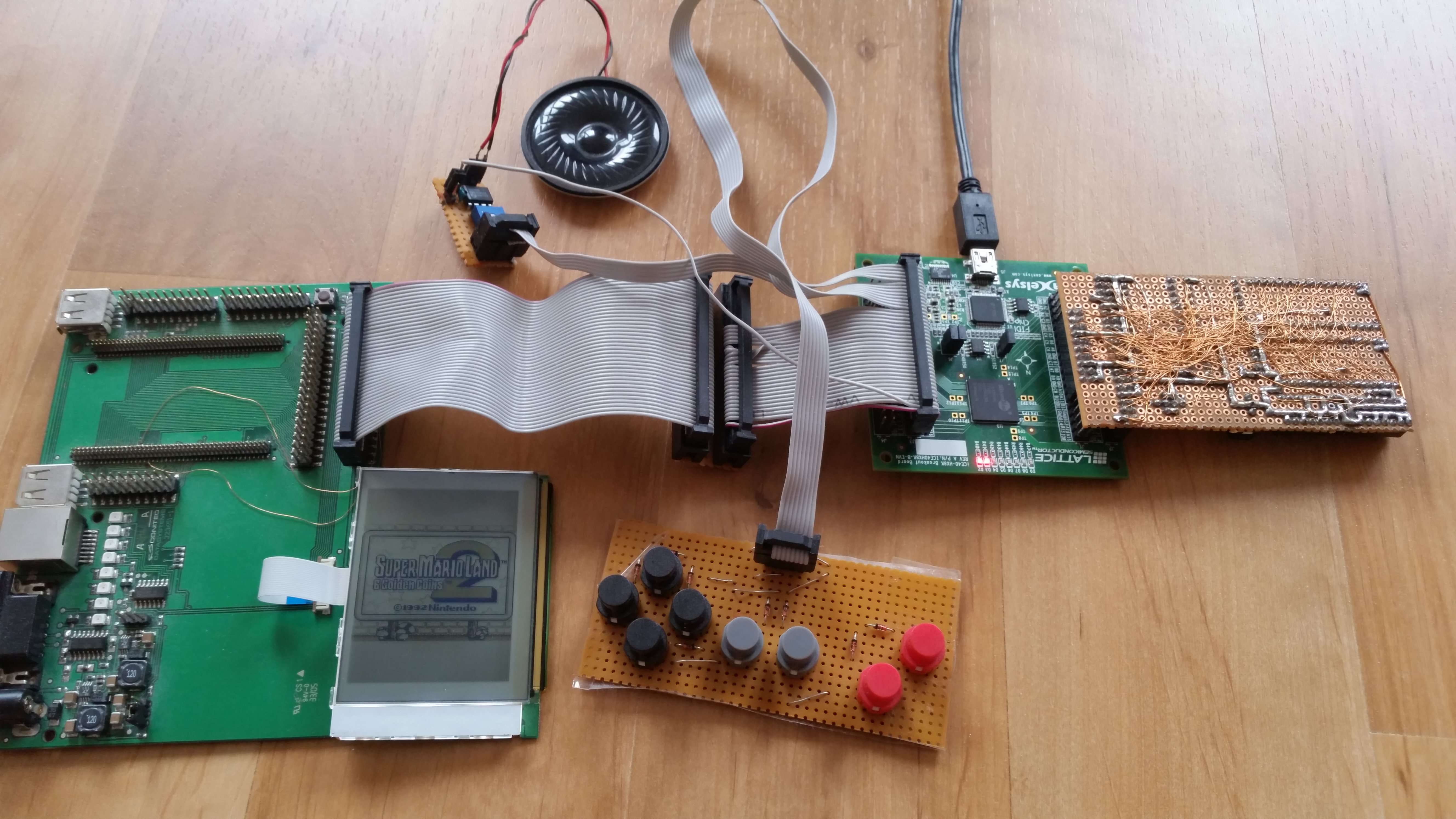
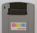
The first prototype was running on a
iCE40-HX8K
Breakout Board with a perfboard attached to it for memory, and a LCD display with UC1611 driver that I got with an
ARM evaluation board
over a decade ago.
The evaluation board on the left side is just used as an adapter to connect the pin header to the small 0.5 mm
pitched connector of the LCD, and also as a power supply. The perfboard on the right side contains SRAM chips: One
for the Game Boy its work RAM, one for the cartridge save game RAM (32 KiB), and two for holding a ROM file (2x512 KiB).
The ROM file can be received over UART while the IceBoy is under reset. The video RAM and boot ROM are FGPA internal.
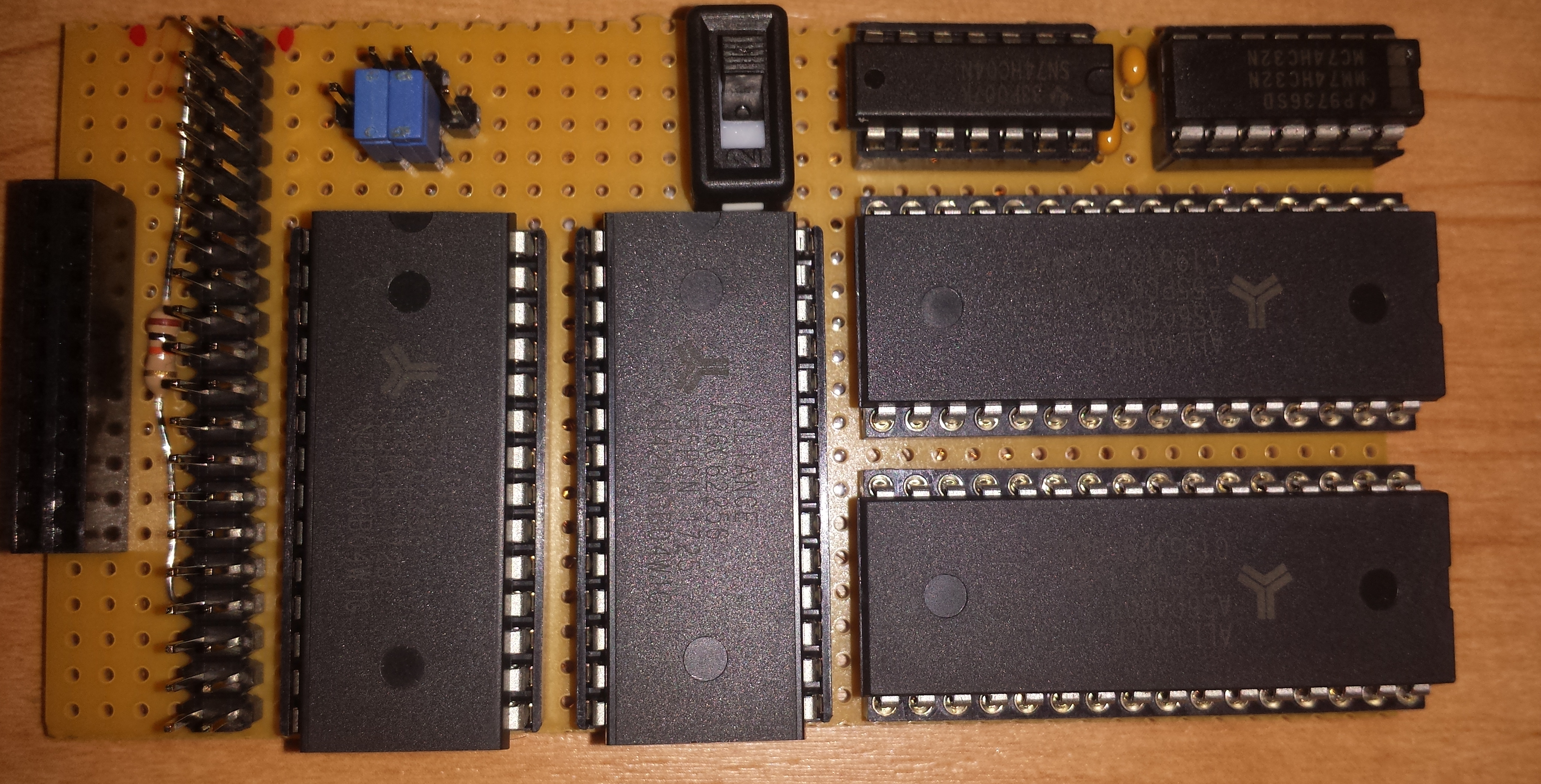
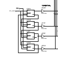
This setup was very fragile so I wanted to make my own PCB for further development. I also wanted a system for making
research on the Game Boy more comfortable. I combined those two aspects into one PCB: The Game Boy reverse engineering
FGPA board.

I let SeeedStudio manufacture and assemble two of those PCBs.
I used their PCB manufacturing services multiple times now and so far I'm very happy with their quality. The board has
all the memory the Game Boy needs onboard. It has even more than the perfboard had. There's 2x1 MiB for the ROM file,
128 KiB for the cartridge RAM and I had added another RAM that has it's own data and address bus, so it can be used as
video RAM. There is a cartridge connector at the top, which can be used instead of loading a ROM file over UART. Just
like on the real Game Boy, the cartridge connector is also sharing its data and address bus with the work RAM. The big
pin header at the far left edge of the PCB can be connected to a real Game Boy using the
GB-BRK-CART v4.0 adapter PCB from Gekkio. The FPGA board can act
as a cartridge to the real Game Boy in this use case. On the right side there is a Game Boy Link Port and in the
bottom right corner a DMG-LCD PCB can be connected with the original 21 pin flex cable, so IceBoy can drive the original
LCD and also sense the buttons and use the original speaker for audio output.
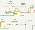
The KiCad project for the board is here:
→ Game Boy reverse
engineering FPGA board KiCad project
→ Game Boy reverse engineering FPGA board schematics PDF
(rev 0)
Game Boy research
I've done a bit of research on Game Boys that I've documented on separate pages:
 |
Game Boy Memory Access Patterns
This is just some basic stuff like what's visible on the external bus when the Game Boy accesses different
address ranges. |
 |
Skip write to 0xff50 register before leaving boot ROM
Of course I wanted to experiment on the boot ROM skip like everybody else did already. I found out which single
clock tick needs to be shortened for the CPU to make a deterministic jump to one specific address. |
 |
Wide-Boy64 Research
I have reverse engineered the schematics of the Wide-Boy64 AGB and was able to dump the Spartan bitstream from
the PROM. |
 |
Weird DMG-CPU Reset Behaviour
I discovered that some state of the clock generation logic inside the DMG-CPU B chip is not properly reset, which
is actually measurable from outside the chip. |
 |
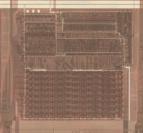
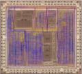
DMG-CPU B Schematics
Régis and I (hopefully) fixed all the bugs left in
Furrtek's schematics and created our own
repository containing KiCad files of Game Boy DMG-CPU B
schematics. Régis did by far most of the work here, putting a lot of effort into a hierarchical structure that
actually makes sense. With only a few exceptions, we kept the cell names given by Furrtek.
|
 |
DMG-CPU SM83 Connections
Here I'm trying to figure out the purpose of each connection from/to the CPU core inside the DMG-CPU B. I use our
schematics and some Icarus Verilog
simulations for that. |
Tools for Game Boy research
During my research attempts, I made some stuff to make further research easier for myself. Maybe it helps you too:
 |
Game Boy Database
A database of all the Game Boys and cartridges I've collected. I stole this idea from Gekkio, there's really no other
way to put it. Check out his huge database. It helped me a lot tracking down
all the different CPU revisions on ebay, based on the serial numbers on the back. |
 |
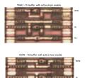
Game Boy DMG-CPU B Map
A Leaflet map of the
DMG-CPU B die shot with our
fixed version of
Furrtek's overlays. The overlays can be switched on and off
and you can actually choose between two versions of the die shot. There's a search box in the bottom left corner where
you can enter the names of the cells or wires, so you don't have to search them manually. |
 |
DMG-CPU Cells Reference
This is supposed to be a complete "reference manual" for all the cells used inside the DMG-CPU B chip. |
TODOs
- IceBoy
- Fix APU channel 1 frequency sweep
- Suppress the final tick of the pixel clock at the end of each line, so the "Funny Playing" display kit also works
- Integrate findings from simulating our DMG-CPU B schematics
- Implement External Link Port
- Implement more MBC chips
- Develop PCB that fits into DMG shell
- Wide-Boy64
Reverse engineer WB64AGB schematics - done 2021-07-22Dump WB64AGB PROM (FPGA bitstream) - done 2021-05-13- Dump WB64AGB EEPROM (likely to be empty)
- Desolder and dump WB64AGB Flash (N64 ROM)
- Develop WB64AGB clone
- Find and buy WB64CGB on ebay