Analog audio mixing and volume adjustment in DMG Game Boy chip
I will first describe all the individual analog components, and then describe how to calculate what gets output at the SO1 and SO2 pins. I highly recommend you have the DMG-CPU B schematics at page 24 and the cell reference open at the same time when reading through this, so you get the full picture what I'm talking about.
The die shot images are from siliconpr0n.org.
Please report any errors I made here.
Individual components
Voltage divider
The simplest analog part involved is a voltage divider that generates a 3V bias voltage for amplifiers. The 3V can be determined in two ways:
1. We can measure the length of the resistors:
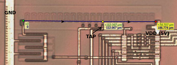
This measurement gives us:
2. We can count the bumps:
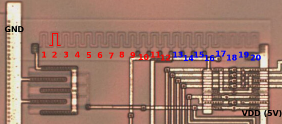
Counting gives us:
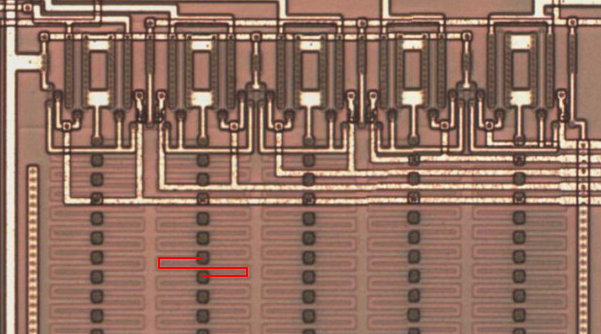
DAC - Digital to analog converter
The DACs are basically just bigger strips of the same "resistor bumps" as we have seen in the voltage divider above, but with multiple taps. On each tap, there is a series of transmission gates that control which tap is actually being used. For pictures and schematics of the DAC, please click here to switch over to the cell reference documentation. In addition to its primary function of converting digital signals to analog, the DACs also have a tap at 2.2V. This 2.2V tap is only used on the DAC of channel 2. The other three channels also have this tap, but it is not connected. The 2.2V are used as reference voltage for the amplifiers that do the volume adjustment.
To determine the voltages at all the different taps of the DACs, I counted the bumps like for the voltage divider. In the schematic of the DAC, each resistor symbol represents exactly one bump. Measuring the length of the resistors would be much harder here, because they are not placed on one straight line.
Here is a table of all possible outputs:
| Digital input D[0..3] | Analog output |
|---|---|
| 0 (0b0000) | 0.7V |
| 1 (0b0001) | 0.9V |
| 2 (0b0010) | 1.1V |
| 3 (0b0011) | 1.3V |
| 4 (0b0100) | 1.5V |
| 5 (0b0101) | 1.7V |
| 6 (0b0110) | 1.9V |
| 7 (0b0111) | 2.1V |
| 8 (0b1000) | 2.3V |
| 9 (0b1001) | 2.5V |
| 10 (0b1010) | 2.7V |
| 11 (0b1011) | 2.9V |
| 12 (0b1100) | 3.1V |
| 13 (0b1101) | 3.3V |
| 14 (0b1110) | 3.5V |
| 15 (0b1111) | 3.7V |
It is a linear mapping that can also be expressed as:
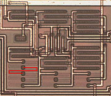
Mixer
The mixer consists of five equal sized resistors that are all connected at one end. Each of the five resistors can be individually deattached by a transmission gate. For pictures and schematics of the mixer, please click here to switch over to the cell reference documentation.
Each of the five resistors is exactly 32 of those S-shaped units long:
RV - Adjustable resistor
The RV cell implements a resistor that can be digitally adjusted in eight steps. It uses transmission gates to bridge parts of its resistance based on the given input. For pictures and schematics of the RV cell, please click here to switch over to the cell reference documentation. The elemental resistor units used in this cell have the same size and shape as the ones in the mixer:
The RV cells are used to adjust the final volume of the left and right channel. It gets controlled by the FF24 register. The 3-bit ADJ input of this cell is the complement of the 3-bit value stored in the FF24 register. Here is a table that shows the relation between register value, cell input and resistance:
| FF24 bits[0..2] or bits[4..6] | ADJ[0..2] input | Resistance |
|---|---|---|
| 0 (0b000) | 0b111 | 1 unit |
| 1 (0b001) | 0b110 | 2 units |
| 2 (0b010) | 0b101 | 3 units |
| 3 (0b011) | 0b100 | 4 units |
| 4 (0b100) | 0b011 | 5 units |
| 5 (0b101) | 0b010 | 6 units |
| 6 (0b110) | 0b001 | 7 units |
| 7 (0b111) | 0b000 | 8 units |
So you just add +1 to the FF24 register fields to get the number of resistor units.
Amplifier
For pictures and schematics of the amplifier, please click here. Due to my limited understanding of analog electronics, I can't really tell what type of amplifier this is. But I can try to explain what it does: The amplifier tries to regulate its output based on the voltage difference at its inputs. If the positive (+) input is higher than its negative (-) input, then the voltage at the output rises. If the positive input is lower than the negative input, the output falls. Of course, I didn't know this at first. I figured it out by simulating the circuit. I will show the simulation results further below, but first I'll explain the basics. Here a piece of schematic how the amplifier is used in most cases:
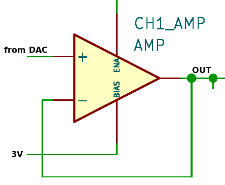
In this scenario, the amplifier basically just replicates the input voltage at its output. I believe this is what pros call a "voltage follower" or "buffer amplifier". The output is fed back to the negative input, and the amplifier regulates its output based on the difference of the inputs. So naturally it is only satisfied when both inputs are equal. And since the output is connected to the negative input, the output needs to be equal as well. We will see in the simulation that this breaks down in edge cases, but for the most part it works.
Don't mind the 3V bias input for now. It needs to be 3V. We will see that this is just the right value when playing with the simulation below.
For volume adjustment, the amplifier is used differently:
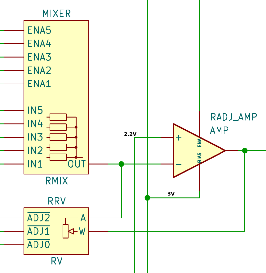
This looks way more complicated, but we can simplify it to make it easier to understand. We simplify it for the following scenario:
- We assume that the four digital APU channels are enabled and the analog VIN channel is disabled.
- Most importantly: We assume that all four channels are outputting the exact same voltage.
- We also assume that the volume is set to 7 (max volume).
You will see in a minute why this specific scenario is so beautifully simple. This would be the equivalent circuit for the described scenario:
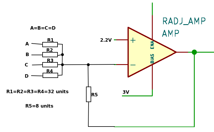
If you are wondering where the "32 units" and "8 units" come from, then please read the description about the mixer and RV cells above.
People with a trained eye in binary numbers will quickly see the relation of the numbers 32 and 8 here. And if those same people also know how to calculate the value of parallel resistors, then they know that we can simplify this even more:
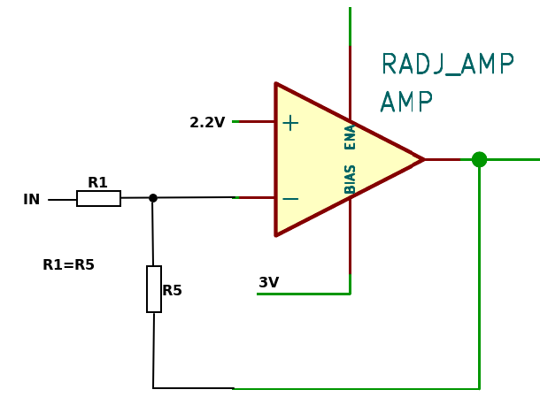
We got a symmetric voltage divider. So let's remember what the amplifier does. It tries to equalize its inputs. The positive input is at fixed 2.2V. Let's assume we apply a voltage of 2.0V at the IN label. In this case, the amplifier needs to output a voltage of 2.4V so that its negative input (which is at the mid-point of the voltage divider) gets 2.2V as well, because . So this amplifier circuit inverts the input voltage. The point at which the input is mirrored is 2.2V.
Now let's assume the volume was set to 0 (min volume). In this case, the resistor R5 would only be an eighth of R1. This would make the circuit a lot more sensible to changes at the amplifier output. The amplifier only needs to output an eighth of the voltage difference to 2.2V to achieve the 2.2V at its negative input. So if you would plot the output over the input voltage, it would be much more flat, close to 2.2V.
Maybe you noticed already, the 2.2V are exactly the mid-point of the voltage range that the DACs can output: - So this is no coincidence that we invert at this voltage level.
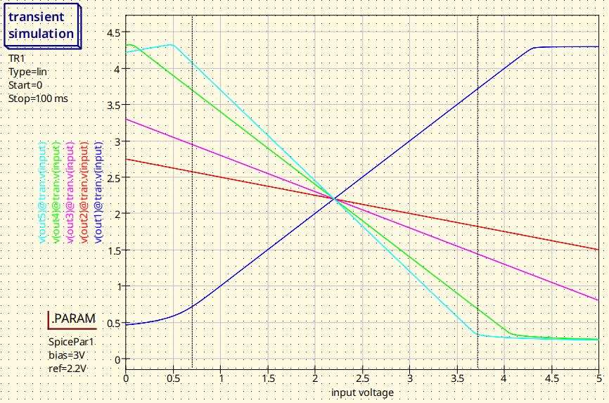
Okay, now that we understand the (in my opinion) easiest scenario of the inverting circuit, let us look at the simulation to get a more generic understanding. I used Qucs-S for simulating. The project consists of two files: amp.sch and sim.sch. This is the circuit in amp.sch:
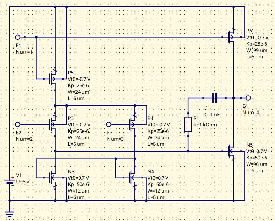
I didn't care about the resistor and capacitor values. I just choose small values so they don't interfere much. I think their purpose is to filter out high noise frequencies or maybe click sounds when switching channels on/off. The length and width properties of the transistors I measured on the die shot. The other transistor properties (Vt0 and Kp) I got from ChatGPT. I asked it to guess some fitting values for technology from that era. From my understanding, those are not that important for getting good simulation results. Getting the relative proportions of width and length correctly is more important. Those decide which transistors are stronger and which ones are weaker than others. You can see, there are transistors competing against each other. E1 is the BIAS input. You see that the 3V bias voltage constantly keeps the output PMOS P6 active to a degree. The output NMOS N5 always has to work against the semi active P6, so I think this is why this is called a bias. But look, for the most part I'm pulling this out of my ass, so take this with a huge grain of salt. E2 is the positive input, E3 is the negative input. And of course, E4 is the output. I didn't bother to include the enable circuit in the simulation. I'm not pretending that I understand how this circuit works. I only know what it does because of the colorful diagrams the simulation spat out. On this territory, I'm a dummy. Dummy dumm dumm.
And here is the other part of the simulation where the amplifier gets used, sim.sch:
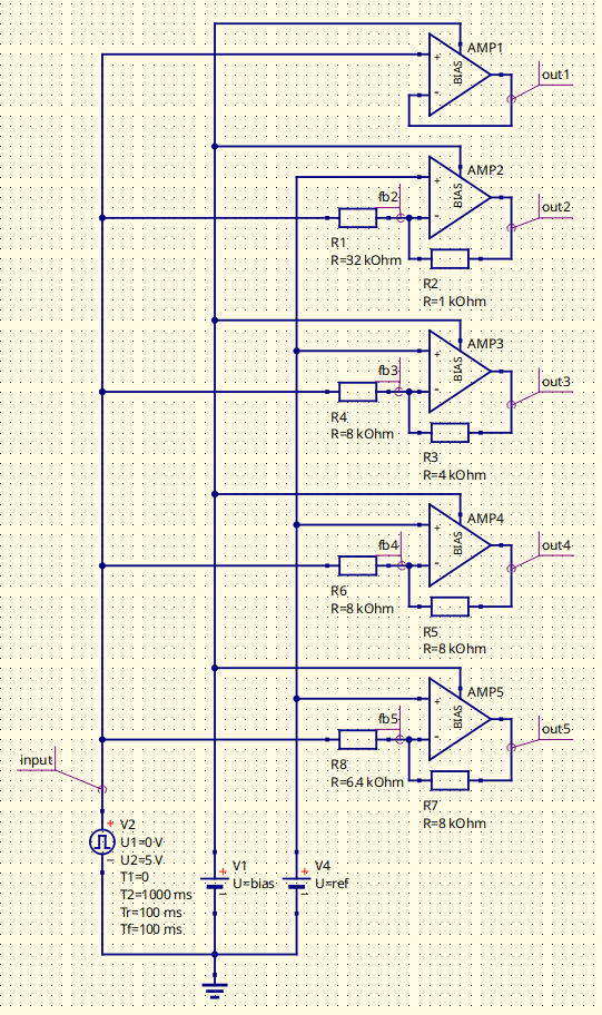
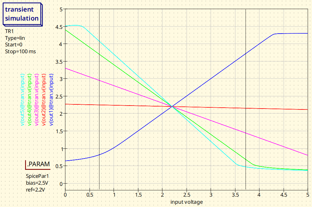
The 3V bias is provided by V1. V4 provides the 2.2V reference for the inverting amplifier scenarios. The pulse thingy V2 is there to run a voltage ramp from 0V to 5V at the amplifier inputs so we can plot every possible input value in a diagram (see below). Then we have five amplifiers as test subjects. Each of them demonstrating a slightly different scenario:
| Amplifier | Scenario |
|---|---|
| AMP1 | The easy voltage follower case where output voltage equals input voltage. |
| AMP2 | Inverting case: Only one channel is enabled, hence R1=32kOhm (I just mapped 1 unit to 1kOhm). Volume is set to 0, hence R2=1kOhm. This should give the flattest possible output in the diagram (except for the case where all channels are disabled). |
| AMP3 | Inverting case: Four channels are enabled, assuming the edge case that all channels provide the same voltage, hence R4=8kOhm. Volume is set to 3, hence R3=4kOhm. |
| AMP4 | Inverting case: Same as AMP3, but volume is set to 7, hence R5=8kOhm. This is the scenario we looked into before, where both resistors are equal. |
| AMP5 | Inverting case: All five channels are enabled, assuming the edge case that all channels provide the same voltage, hence R8=6.4kOhm. Volume is set to 7, hence R7=8kOhm. So this should give us the absolute minimum and maximum outputs. |
Finally, let's plot the diagram:
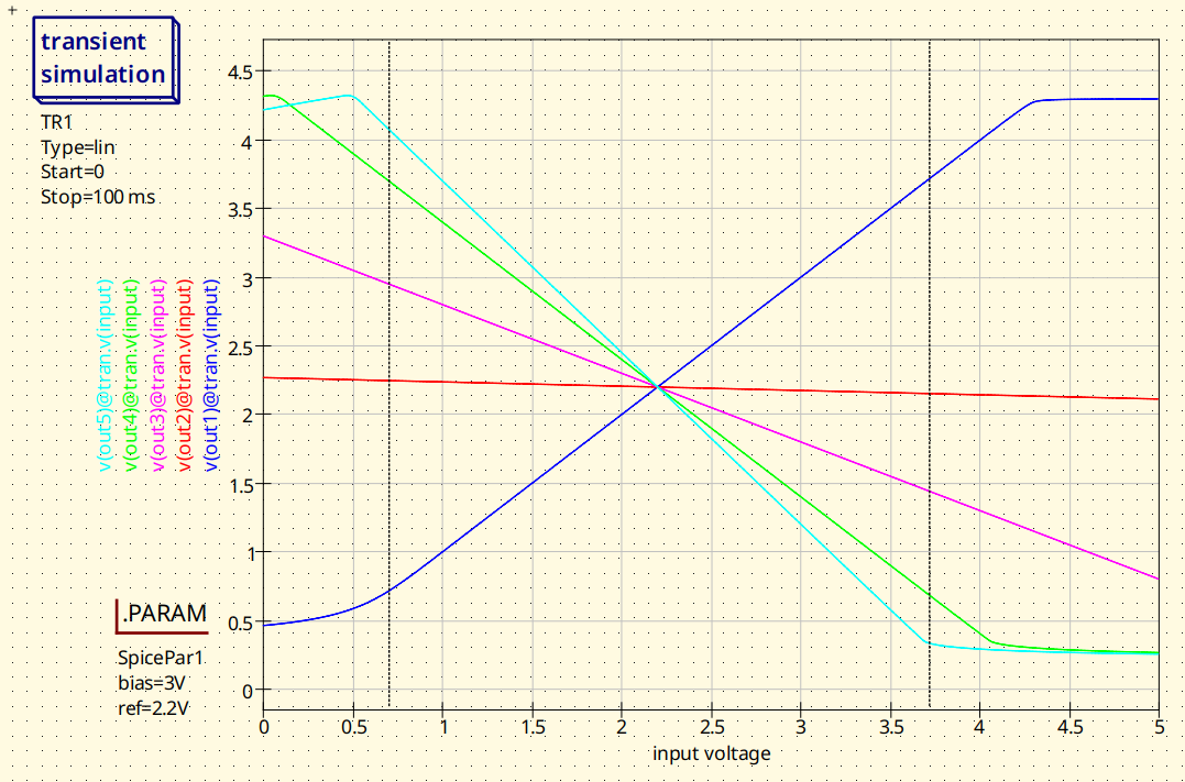
The X axis is the input voltage that gets ramped through by V2. I added dotted vertical lines at 0.7V and 3.7V, which are the min and max values that the DACs can provide. We see that everything is nicely linear within that range, except for a small piece at the bottom right of the cyan output.
What I'd like to point out is that in the green case (AMP4), the inversion maps perfectly into the same range of values: 0.7V maps to 3.7V, and 3.7V maps to 0.7V. This is the case when all four "normal" APU channels are enabled, all provide the same voltage, and the volume is set to max. So if we don't support VIN in an emulator or simulator, then we will never leave the 0.7V-3.7V range. The cyan plot however, where all five channels are enabled, breaks out of that range. And theoretically, VIN is not necessarily restricted to 0.7V-3.7V anyway, since it comes from an external source. It could be 0V-5V, and break things even more.
Out of curiosity, I also plotted the negative inputs of the inverting amps:
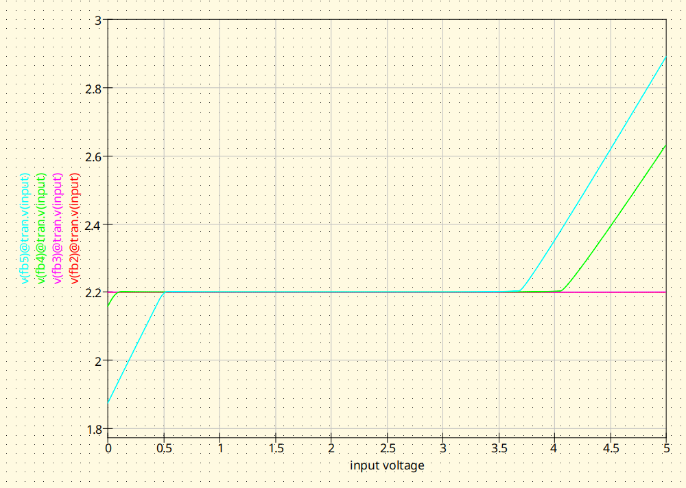
We can see how the amplifiers keep their inputs equal, except in the extreme cases for green and cyan.
Now let's try what happens when we change the bias voltage to 2.5V:
We see that the window in which things behave linear shrinks. The dark blue line gets bent at the bottom, and the cyan also looses more linearity than before at the bottom.
Let's change the bias into the other direction, to 3.5V:
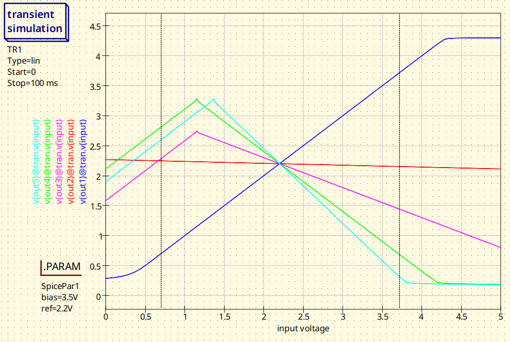
Yeah, maybe we just don't talk about that. I think it's pretty obvious why this is not good.
How to calculate the voltages
Calculating the analog voltages for the four APU channels is the easiest thing. Each channel's output is represented by a 4-bit digital value. In the schematics those are named chn_out. The output of the individual channel amplifiers is always the same as the output of their DACs, since they are configured as voltage followers, so we can directly calculate the amplifier outputs chn_amp_out:
Mixing and volume adjustment is a little bit trickier, because of the resistors involved and the fact that channels can be enabled/disabled. Channels can be enabled/disabled directly at the mixer, simply by using the FF25 register for channels 1-4, and by bit 3 and 7 of the FF24 register for VIN. Those two registers directly hold the enable signals of the two mixers. There is another way, however, how channels can be enabled/disabled: Their amplifiers get an enable signal from some specific register bits that are different for each channel. Here are the relevant pieces from the schematic:
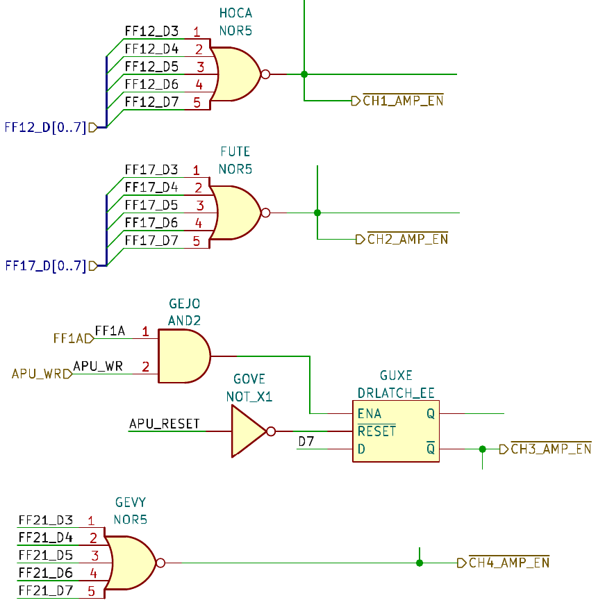
Channels 1, 2 and 4 have their amplifiers enabled when any of the bits 3..7 in registers FF12, FF17 or FF21 respectively are high. Channel 3 has its amplifier enabled when bit 7 in register FF1A is high.
When an amplifier is disabled, its output is undriven (high-z). This has the same effect as if the respective mixer input is disabled, so we can just throw both conditions together in one equation per channel:
I use those boolean enable signals like integers that are either 0 or 1 in the equations below. We now have everything we need to be able to calculate the RADJ_AMP and LADJ_AMP outputs like this:
We have to subtract 2.2V from all input voltages, so that we can invert the signals at this voltage level. At the end we add the 2.2V again. Each of the five mixer inputs gets multiplied by 0.25, because, like we have seen in my favorite scenario that I described multiple times above (AMP4, the one where both resistors of the divider are equal), we need four mixer inputs to reach exactly the same voltage range at input and output (0.7V-3.7V), because .
The final output should be restricted between ~0.3V and ~4.3V as can be seen in the simulation plot.
The analog circuit as a whole will only be enabled when at least one of the four APU channels is enabled:
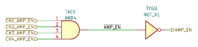
So this must be true, otherwise the analog outputs will be undriven (high-z):
This also implies that VIN can't be enabled on its own. At least one of the four channels needs to be enabled. (They don't need to be enabled in the mixer though.)
If amp_en is true, but all five channels are disabled in the mixer, the final output is 2.2V, because 2.2V are applied to {R,L}ADJ_AMPs positive input.
Testing and comparison with reality
The coin sound that plays when the Nintendo logo hits the center of the screen looks like this in the Verilog simulation:
In this scenario, only channel 1 is enabled. When channel 1 is idle (not playing a sound, but is enabled), you see that its resting level is at 0.7V, because it inputs 0b0000 into its DAC. The left mixer output (ladj) and the analog output pin of the chip (lout) both read as 2.575V when channel 1 is enabled and idle. This is due to the inverting and scaling that happens at LADJ_AMP. Since we didn't have this scenario before, I quickly changed R2 in the spice sim to 8kOhm. The red line now shows channel 1 alone at full volume:
We can see with 0.7V input, it outputs ~2.6V.
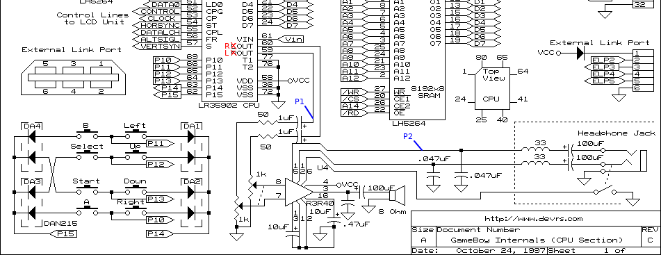
So far so good. Now let's test this in real life. I attached my oscilloscope probes to the points P1 and P2 of the main PCB:
Headphones must be plugged in, otherwise there will be no signal at P2.
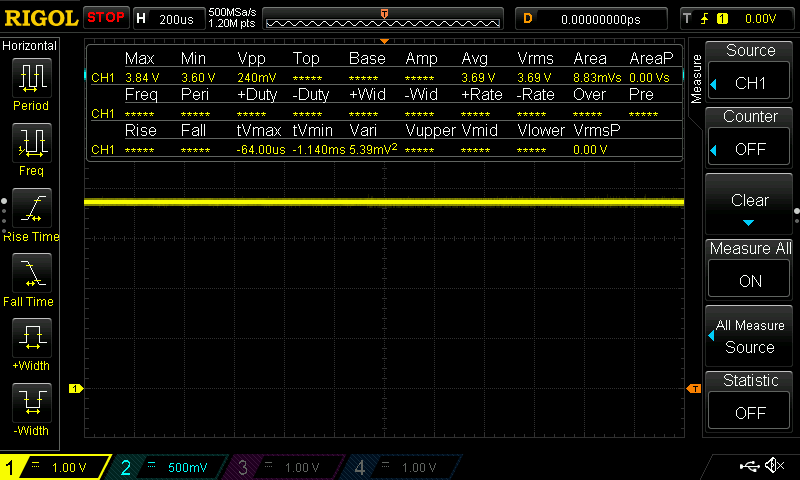
While no sound is playing and only channel 1 is enabled, we see this:
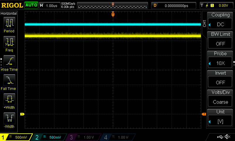
The yellow signal is at P1, the blue one is at P2. At P2 (after the DMG-AMP chip) the signal always has this huge offset and, like we will see further below, is much more flat. But the thing I was interested in why I attached P2: The signal is not inverted by the external amp. Let's display some measurements:
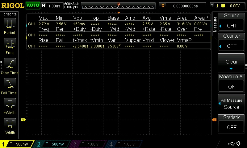
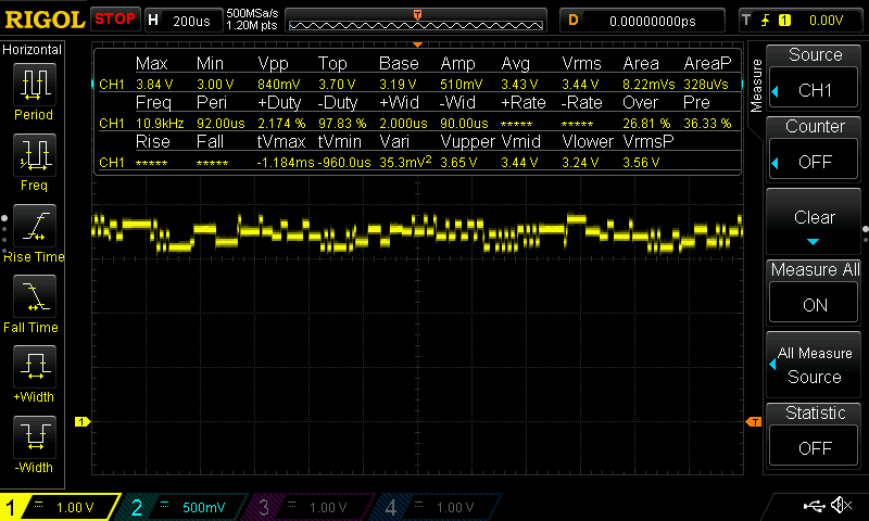
We see that the average voltage at P1 is somewhere at ~2.6V which fits our calculations for an idle channel 1. Now we let the coin sound play:

Like our calculations and the simulation predicts, the voltage alternates between the ~2.6V idle state and some lower state which depends on the current digital volume of channel 1. (I didn't use any triggers, I just pressed stop when it started moving.)
Now I started Zelda, from which I know that it enables all four channels during the animations before the title screen. I waited until Link's ship got destroyed, just before he was washed ashore. There is a short moment of silence:
We see the idle voltage is much higher, at ~3.7V, when four channels are enabled. Exactly how we predicted with our calculations.
Here is the sound of the waves:
The upper voltage level stays at the ~3.7V. It can't go up any further, because that's not possible with only four channels, like we see in our spice diagrams above. But it can go down. It is very unlikely to reach the 0.7V bottom, because for this, all four channels would need to be at full volume and output 3.7V.
And here is some high-end premium Zelda music playing:
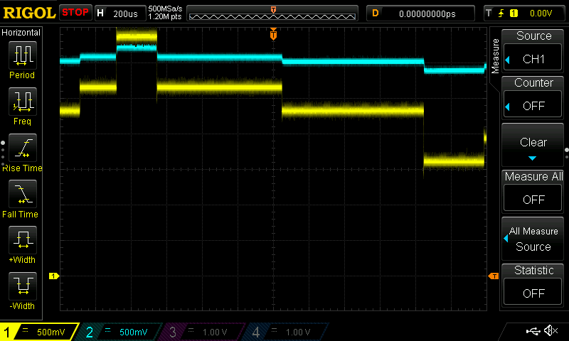
It reaches much lower voltages. I think because it is louder.
I think what we see fits the simulations.