IceBoy - Game Boy clone and research

This domain serves as a place for documenting the progress of developing my Game Boy clone (IceBoy) and all the stuff I found out about the real Game Boys. I started with IceBoy because I wanted to learn about FPGAs and thought a Game Boy would be a fun project for that. I decided to develop IceBoy for the Lattice iCE40 FPGA family. This is where the name IceBoy comes from: iCE40 → IceBoy. I made this decision to use the iCE40 family because I wanted to use a toolchain that is completely open source: Project IceStorm.

You can find further details about IceBoy here.

Game Boy research

I've done a lot of research on Game Boys that I've documented on separate pages:

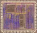
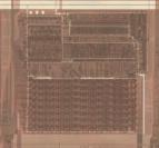
DMG-CPU B Schematics
SM83 Schematics
Régis and I (hopefully) fixed all the bugs left in Furrtek's schematics and created our own repository containing KiCad files of Game Boy DMG-CPU B schematics. Régis did by far most of the work here, putting a lot of effort into a hierarchical structure that actually makes sense. With only a few exceptions, we kept the cell names given by Furrtek.
The schematics of the SM83 CPU core and all the analog audio circuitry, which were not covered previously, are now also available.
DMG-CPU Cells Reference
SM83 Cells Reference
These ought to be "reference manuals" for all the cells used inside the DMG-CPU B chip and the SM83 CPU core. I highly recommend to read these whenever the exact function of individual cells inside the schematics above are unclear or if you need more information. Most cells are documented with their own transistor level schematic and annotated layouts.
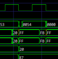
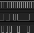
DMG-CPU SM83 Connections
Here I described the purpose of each input/output of the SM83 CPU core inside the DMG-CPU B chip. I used our schematics and the Icarus Verilog simulations for that.
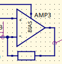
Wide-Boy64 Research
I have reverse engineered the schematics of the Wide-Boy64 AGB and was able to dump the Spartan bitstream from the PROM and also the N64 code from the flash.
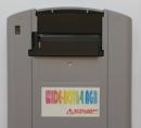
Nintendo Power Game Boy Memory cartridge documentation
I have documented how to fully read, erase and program the white flash cartridges.

Tools for Game Boy research

During my research attempts, I made some stuff to make further research easier for myself. Maybe it helps you too:

Game Boy DMG-CPU B Map
SM83 Map
Leaflet maps of DMG-CPU B die shots and more detailed pictures of the SM83 CPU core. Source images are taken from siliconpr0n.org, Gekkio and emu-russia/ogamespec.
Icarus Verilog simulation
A simulation of the complete DMG-CPU B chip that strives to reproduce all signal timings as close to the original as possible. Helps to explain many of the bugs and glitches of the chip.
Visual SM83 Transistor Level Simulation in JavaScript
A port of visual6502.org for the Game Boy CPU.
Game Boy Database
A database of all the Game Boys and cartridges I've collected. I stole this idea from Gekkio, there's really no other way to put it. Check out his huge database. It helped me a lot to track down all the different CPU revisions on eBay, based on the serial numbers on the back.

Older Game Boy research

Here some older research that I've done before we had the schematics and the simulation for explanations:

Game Boy Memory Access Patterns
This is just some basic stuff like what's visible on the external bus when the Game Boy accesses different address ranges.
Skip write to 0xff50 register before leaving boot ROM
Of course, I wanted to experiment on the boot ROM skip like everybody else did already. I found out which single clock tick needs to be shortened for the CPU to make a deterministic jump to one specific address.
Weird DMG-CPU Reset Behavior
I discovered that some state of the clock generation logic inside the DMG-CPU B chip is not properly reset, which is actually measurable from outside the chip.