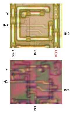
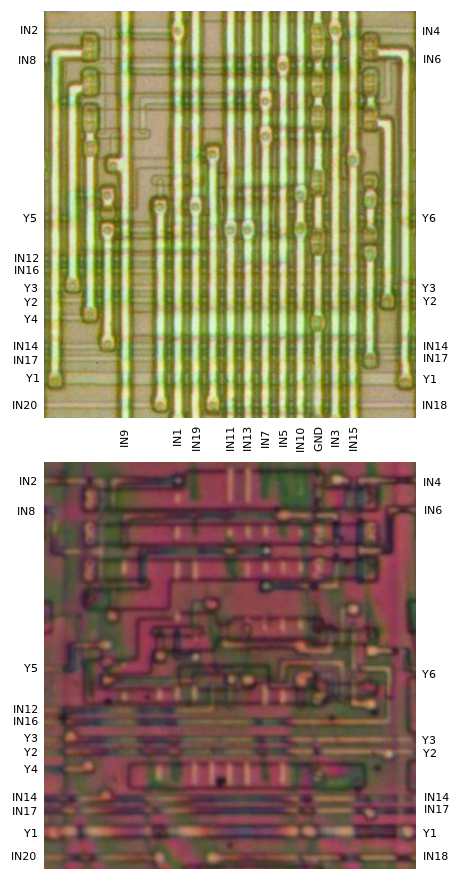
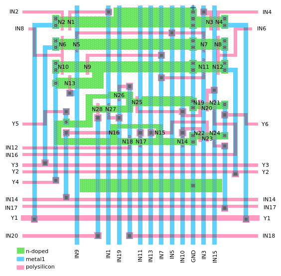
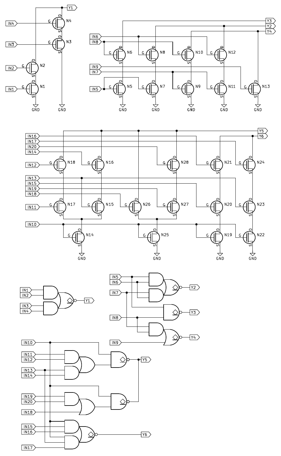
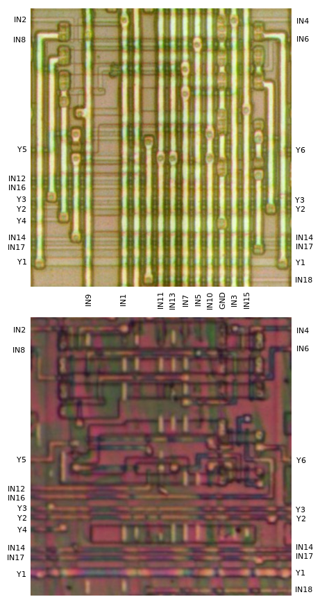
SM83 Cells Reference
This document provides information about the cells found in the SM83 CPU core of the Game Boy.
Please report any errors I made here.
Basic logic gates
NOT gates
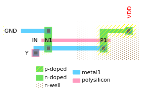
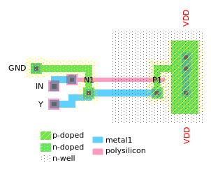
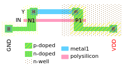
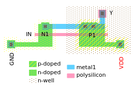
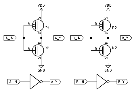
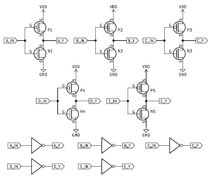
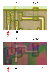
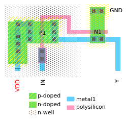
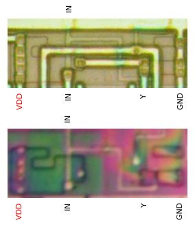
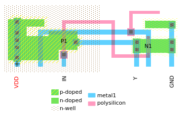
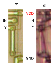
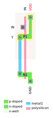
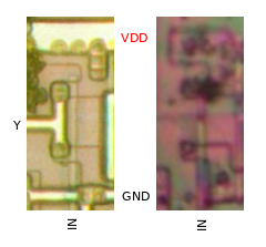
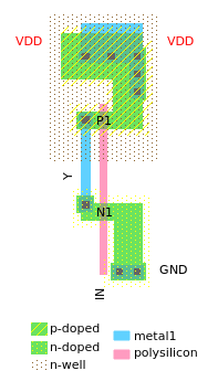
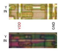
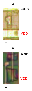
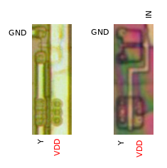
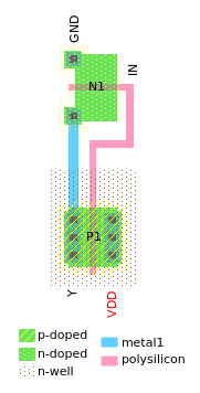
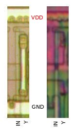
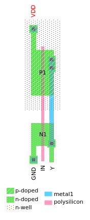
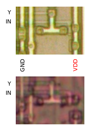
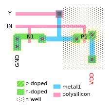
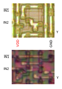
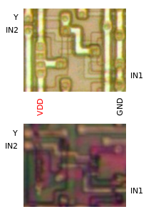
NOT_A
Simple inverter.
 |
| I/O | Description |
|---|
| IN |
Input to inverter. |
| Y |
Outputs inverted IN. |
|
Instances:
ZGNA
(1 total)
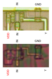
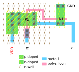
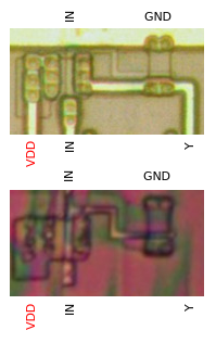
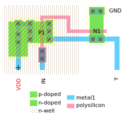
NOT_B
Simple inverter.
 |
| I/O | Description |
|---|
| IN |
Input to inverter. |
| Y |
Outputs inverted IN. |
|
Instances:
ZUDN
(1 total)
NOT_C
Simple inverter.
 |
| I/O | Description |
|---|
| IN |
Input to inverter. |
| Y |
Outputs inverted IN. |
|
Instances:
YEPJ
(1 total)
NOT_D
Simple inverter.
 |
| I/O | Description |
|---|
| IN |
Input to inverter. |
| Y |
Outputs inverted IN. |
|
Instances:
XURI
(1 total)
NOT_E
Simple inverter.
 |
| I/O | Description |
|---|
| IN |
Input to inverter. |
| Y |
Outputs inverted IN. |
|
Instances:
XWEE
(1 total)
NOT_F
Simple inverter.
 |
| I/O | Description |
|---|
| IN |
Input to inverter. |
| Y |
Outputs inverted IN. |
|
Instances:
XUDO
(1 total)
NOT_G
Simple inverter.
 |
| I/O | Description |
|---|
| IN |
Input to inverter. |
| Y |
Outputs inverted IN. |
|
Instances:
ZKON
(1 total)
NOT_X3_P2
Inverter with 3× drive strength and a PMOS-to-NMOS size ratio of 2:1.
 |
| I/O | Description |
|---|
| IN |
Input to inverter. |
| Y |
Outputs inverted IN. |
|
Instances:
ZJBF
(1 total)
NOT_REG
Simple inverter.
 |
| I/O | Description |
|---|
| IN |
Input to inverter. |
| Y |
Outputs inverted IN. |
|
Instances:
REG_NOT[0],
REG_NOT[1],
REG_NOT[2],
REG_NOT[3],
REG_NOT[4],
REG_NOT[5],
REG_NOT[6],
REG_NOT[7]
(8 total)
NOT2_IDU
Two simple inverters.
 |
| I/O | Description |
|---|
| A_IN |
Input to inverter A. |
| A_Y |
Outputs inverted A_IN. |
| B_IN |
Input to inverter B. |
| B_Y |
Outputs inverted B_IN. |
|
Instances:
IDU_NOT[0],
IDU_NOT[1],
IDU_NOT[2],
IDU_NOT[3],
IDU_NOT[4],
IDU_NOT[5],
IDU_NOT[6],
IDU_NOT[7]
(8 total)
NOT5_IRQ
Five simple inverters.
 |
| I/O | Description |
|---|
| A_IN |
Input to inverter A. |
| A_Y |
Outputs inverted A_IN. |
| B_IN |
Input to inverter B. |
| B_Y |
Outputs inverted B_IN. |
| C_IN |
Input to inverter C. |
| C_Y |
Outputs inverted C_IN. |
| D_IN |
Input to inverter D. |
| D_Y |
Outputs inverted D_IN. |
| E_IN |
Input to inverter E. |
| E_Y |
Outputs inverted E_IN. |
|
Instances:
IRQ_HEAD
(1 total)
NOT_REG_WE
Simple inverter.
 |
| I/O | Description |
|---|
| IN |
Input to inverter. |
| Y |
Outputs inverted IN. |
|
Instances:
REG_C_NOT_WE,
REG_D_NOT_WE,
REG_IR_NOT_WE,
REG_W_NOT_WE,
REG_Z_NOT_WE
(5 total)
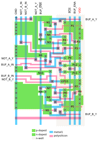
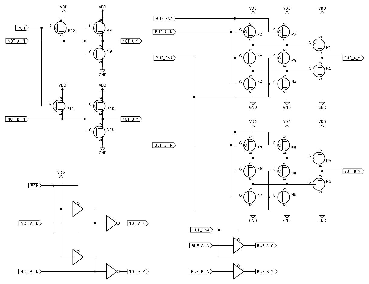
NOT_REG_A_WE
Simple inverter.
 |
| I/O | Description |
|---|
| IN |
Input to inverter. |
| Y |
Outputs inverted IN. |
|
Instances:
REG_A_NOT_WE
(1 total)
NOT_REG_B_WE
Simple inverter.
 |
| I/O | Description |
|---|
| IN |
Input to inverter. |
| Y |
Outputs inverted IN. |
|
Instances:
REG_B_NOT_WE
(1 total)
NOT_REG_H_E_WE
Simple inverter.
 |
| I/O | Description |
|---|
| IN |
Input to inverter. |
| Y |
Outputs inverted IN. |
|
Instances:
REG_E_NOT_WE,
REG_H_NOT_WE
(2 total)
NOT_REG_IE_WE
Simple inverter.
 |
| I/O | Description |
|---|
| IN |
Input to inverter. |
| Y |
Outputs inverted IN. |
|
Instances:
REG_IE_NOT_WE
(1 total)
NOT_REG_L_WE
Simple inverter.
 |
| I/O | Description |
|---|
| IN |
Input to inverter. |
| Y |
Outputs inverted IN. |
|
Instances:
REG_L_NOT_WE
(1 total)
NOT_REG_SP_WE
Simple inverter.
 |
| I/O | Description |
|---|
| IN |
Input to inverter. |
| Y |
Outputs inverted IN. |
|
Instances:
REG_SPH_NOT_WE,
REG_SPL_NOT_WE
(2 total)
NOT2_REG_PC_WE
Two simple inverters.
 |
| I/O | Description |
|---|
| A_IN |
Input to inverter A. |
| A_Y |
Outputs inverted A_IN. |
| B_IN |
Input to inverter B. |
| B_Y |
Outputs inverted B_IN. |
|
Instances:
REG_PCH_NOT_WE,
REG_PCL_NOT_WE
(2 total)
NOT_ALU_A
Simple inverter.
 |
| I/O | Description |
|---|
| IN |
Input to inverter. |
| Y |
Outputs inverted IN. |
|
Instances:
ALU_NOT11
(1 total)
NOT_ALU_B
Simple inverter.
 |
| I/O | Description |
|---|
| IN |
Input to inverter. |
| Y |
Outputs inverted IN. |
|
Instances:
ALU_NOT12
(1 total)
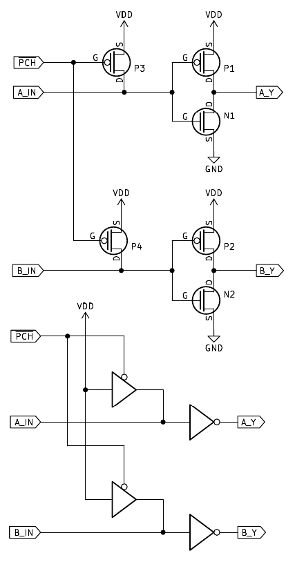
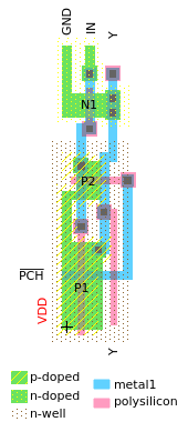
NOT_PCH_X1_ALU
Inverter with precharge.
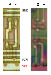 |
| I/O | Description |
|---|
| IN |
Input to inverter. Outputs high if PCH is low. |
| Y |
Outputs inverted IN. |
| PCH |
Active-low precharge input. If low, IN gets driven high for the purpose of precharging the net
connected to the input. |
|

Instances:
ALU_NOT9
(1 total)
NOT_PCH_X2_ALU
Inverter with precharge. Precharge has 2× drive strength.
 |
| I/O | Description |
|---|
| IN |
Input to inverter. Outputs high if PCH is low. |
| Y |
Outputs inverted IN. |
| PCH |
Active-low precharge input. If low, IN gets driven high for the purpose of precharging the net
connected to the input. |
|
Instances:
ALU_NOT1,
ALU_NOT2,
ALU_NOT3,
ALU_NOT4,
ALU_NOT5,
ALU_NOT6,
ALU_NOT7,
ALU_NOT8,
ALU_NOT10
(9 total)
NOT_DEC1
Simple inverter.
 |
| I/O | Description |
|---|
| IN |
Input to inverter. |
| Y |
Outputs inverted IN. |
|
Instances:
DEC1_NOT55,
DEC1_NOT56,
DEC1_NOT57,
DEC1_NOT58,
DEC1_NOT59,
DEC1_NOT60,
DEC1_NOT61,
DEC1_NOT62,
DEC1_NOT63,
DEC1_NOT64,
DEC1_NOT65,
DEC1_NOT66,
DEC1_NOT67,
DEC1_NOT68,
DEC1_NOT69,
DEC1_NOT70,
DEC1_NOT71,
DEC1_NOT72
(18 total)
NOT_PCH_DEC1
Inverter with precharge.
 |
| I/O | Description |
|---|
| IN |
Input to inverter. Outputs high if PCH is low. |
| Y |
Outputs inverted IN. |
| PCH |
Active-low precharge input. If low, IN gets driven high for the purpose of precharging the net
connected to the input. |
|
Instances:
DEC1_NOT54
(1 total)
NOT2_PCH_DEC1
Two inverters with precharge.
 |
| I/O | Description |
|---|
| A_IN |
Input to inverter A. Outputs high if PCH is low. |
| A_Y |
Outputs inverted A_IN. |
| B_IN |
Input to inverter B. Outputs high if PCH is low. |
| B_Y |
Outputs inverted B_IN. |
| PCH |
Active-low precharge input. If low, A_IN and B_IN get driven high for the purpose of
precharging the nets connected to the inputs. |
|
Instances:
DEC1_NOT1,
DEC1_NOT2,
DEC1_NOT3,
DEC1_NOT4,
DEC1_NOT5,
DEC1_NOT6,
DEC1_NOT7,
DEC1_NOT8,
DEC1_NOT9,
DEC1_NOT10,
DEC1_NOT11,
DEC1_NOT12,
DEC1_NOT13,
DEC1_NOT14,
DEC1_NOT15,
DEC1_NOT16,
DEC1_NOT17,
DEC1_NOT18,
DEC1_NOT19,
DEC1_NOT20,
DEC1_NOT21,
DEC1_NOT22,
DEC1_NOT23,
DEC1_NOT24,
DEC1_NOT25,
DEC1_NOT26,
DEC1_NOT27,
DEC1_NOT28,
DEC1_NOT29,
DEC1_NOT30,
DEC1_NOT31,
DEC1_NOT32,
DEC1_NOT33,
DEC1_NOT34,
DEC1_NOT35,
DEC1_NOT36,
DEC1_NOT37,
DEC1_NOT38,
DEC1_NOT39,
DEC1_NOT40,
DEC1_NOT41,
DEC1_NOT42,
DEC1_NOT43,
DEC1_NOT44,
DEC1_NOT45,
DEC1_NOT46,
DEC1_NOT47,
DEC1_NOT48,
DEC1_NOT49,
DEC1_NOT50,
DEC1_NOT51,
DEC1_NOT52,
DEC1_NOT53
(53 total)
NOT_X1_DEC2
Simple inverter.
 |
| I/O | Description |
|---|
| IN |
Input to inverter. |
| Y |
Outputs inverted IN. |
|
Instances:
DEC2_NOT1,
DEC2_NOT2,
DEC2_NOT3,
DEC2_NOT4,
DEC2_NOT5,
DEC2_NOT9,
DEC2_NOT10,
DEC2_NOT11,
DEC2_NOT12,
DEC2_NOT13,
DEC2_NOT14,
DEC2_NOT15,
DEC2_NOT16,
DEC2_NOT19,
DEC2_NOT20,
DEC2_NOT22,
DEC2_NOT23,
DEC2_NOT24,
DEC2_NOT25,
DEC2_NOT26,
DEC2_NOT27,
DEC2_NOT28,
DEC2_NOT29,
DEC2_NOT30,
DEC2_NOT31
(25 total)
NOT_X1_P2_DEC2
Inverter with 2× PMOS drive strength.
 |
| I/O | Description |
|---|
| IN |
Input to inverter. |
| Y |
Outputs inverted IN. |
|
Instances:
DEC2_NOT7,
DEC2_NOT8,
DEC2_NOT17,
DEC2_NOT18
(4 total)
NOT_X1_PCH_DEC2
Inverter with precharge.
 |
| I/O | Description |
|---|
| IN |
Input to inverter. Outputs high if PCH is low. |
| Y |
Outputs inverted IN. |
| PCH |
Active-low precharge input. If low, IN gets driven high for the purpose of precharging the net
connected to the input. |
|
Instances:
DEC2_NOT21
(1 total)
NOT_X2_DEC2
Inverter with 2× drive strength.
 |
| I/O | Description |
|---|
| IN |
Input to inverter. |
| Y |
Outputs inverted IN. |
|
Instances:
DEC2_NOT6
(1 total)
NOT_DEC3
Simple inverter.
 |
| I/O | Description |
|---|
| IN |
Input to inverter. |
| Y |
Outputs inverted IN. |
|
Instances:
DEC3_NOT68
(1 total)
NOT_PCH_DEC3_A
Inverter with precharge.
 |
| I/O | Description |
|---|
| IN |
Input to inverter. Outputs high if PCH is low. |
| Y |
Outputs inverted IN. |
| PCH |
Active-low precharge input. If low, IN gets driven high for the purpose of precharging the net
connected to the input. |
|
Instances:
DEC3_NOT1,
DEC3_NOT2,
DEC3_NOT3,
DEC3_NOT4,
DEC3_NOT5,
DEC3_NOT6,
DEC3_NOT7,
DEC3_NOT8,
DEC3_NOT9,
DEC3_NOT10,
DEC3_NOT11,
DEC3_NOT12,
DEC3_NOT13,
DEC3_NOT14,
DEC3_NOT15,
DEC3_NOT17,
DEC3_NOT18,
DEC3_NOT19,
DEC3_NOT20,
DEC3_NOT21,
DEC3_NOT22,
DEC3_NOT25,
DEC3_NOT32,
DEC3_NOT33,
DEC3_NOT42,
DEC3_NOT43,
DEC3_NOT44,
DEC3_NOT45,
DEC3_NOT46,
DEC3_NOT53,
DEC3_NOT58,
DEC3_NOT59,
DEC3_NOT60,
DEC3_NOT61,
DEC3_NOT62,
DEC3_NOT63,
DEC3_NOT64,
DEC3_NOT65,
DEC3_NOT66,
DEC3_NOT67
(40 total)
NOT_PCH_DEC3_A2
Inverter with precharge.
 |
| I/O | Description |
|---|
| IN |
Input to inverter. Outputs high if PCH is low. |
| Y |
Outputs inverted IN. |
| PCH |
Active-low precharge input. If low, IN gets driven high for the purpose of precharging the net
connected to the input. |
|
Instances:
DEC3_NOT24,
DEC3_NOT31,
DEC3_NOT37
(3 total)
NOT_PCH_DEC3_B
Inverter with precharge.
 |
| I/O | Description |
|---|
| IN |
Input to inverter. Outputs high if PCH is low. |
| Y |
Outputs inverted IN. |
| PCH |
Active-low precharge input. If low, IN gets driven high for the purpose of precharging the net
connected to the input. |
|
Instances:
DEC3_NOT16,
DEC3_NOT30,
DEC3_NOT49,
DEC3_NOT50,
DEC3_NOT51,
DEC3_NOT52,
DEC3_NOT56
(7 total)
NOT_PCH_DEC3_B2
Inverter with precharge.
 |
| I/O | Description |
|---|
| IN |
Input to inverter. Outputs high if PCH is low. |
| Y |
Outputs inverted IN. |
| PCH |
Active-low precharge input. If low, IN gets driven high for the purpose of precharging the net
connected to the input. |
|
Instances:
DEC3_NOT29,
DEC3_NOT38,
DEC3_NOT39,
DEC3_NOT40,
DEC3_NOT41
(5 total)
NOT_P2_DEC3_A
Inverter with 2× PMOS drive strength.
 |
| I/O | Description |
|---|
| IN |
Input to inverter. |
| Y |
Outputs inverted IN. |
|
Instances:
DEC3_NOT69,
DEC3_NOT70,
DEC3_NOT73,
DEC3_NOT74
(4 total)
NOT_P2_DEC3_B
Inverter with 2× PMOS drive strength.
 |
| I/O | Description |
|---|
| IN |
Input to inverter. |
| Y |
Outputs inverted IN. |
|
Instances:
DEC3_NOT71,
DEC3_NOT72
(2 total)
NOT_P2_PCH_DEC3
Inverter with 2× PMOS drive strength, and precharge.
 |
| I/O | Description |
|---|
| IN |
Input to inverter. Outputs high if PCH is low. |
| Y |
Outputs inverted IN. |
| PCH |
Active-low precharge input. If low, IN gets driven high for the purpose of precharging the net
connected to the input. |
|
Instances:
DEC3_NOT23,
DEC3_NOT26,
DEC3_NOT27,
DEC3_NOT28,
DEC3_NOT34,
DEC3_NOT35,
DEC3_NOT36,
DEC3_NOT47,
DEC3_NOT48,
DEC3_NOT54,
DEC3_NOT55,
DEC3_NOT57
(12 total)
NOT_DBUS
Simple inverter.
 |
| I/O | Description |
|---|
| IN |
Input to inverter. |
| Y |
Outputs inverted IN. |
|
Instances:
DBUS_NOT[0],
DBUS_NOT[1],
DBUS_NOT[2],
DBUS_NOT[3],
DBUS_NOT[4],
DBUS_NOT[5],
DBUS_NOT[6],
DBUS_NOT[7]
(8 total)
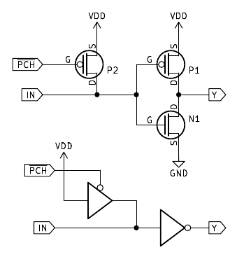
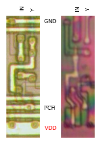
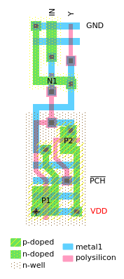
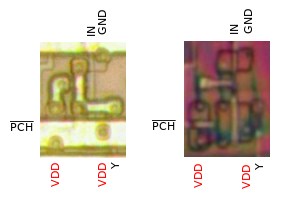
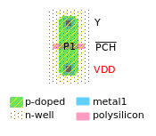
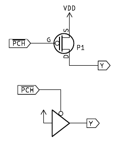
PCH_DEC2_A
Simple PMOS transistor for precharging.
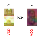 |
| I/O | Description |
|---|
| PCH |
Active-low precharge input. If low, output Y gets driven high. |
| Y |
Outputs high if PCH is low. |
|
Instances:
DEC2_PCH1
(1 total)
PCH_DEC2_B
Simple PMOS transistor for precharging.
 |
| I/O | Description |
|---|
| PCH |
Active-low precharge input. If low, output Y gets driven high. |
| Y |
Outputs high if PCH is low. |
|
Instances:
DEC2_PCH4
(1 total)
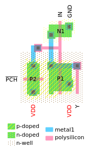
PCH_DEC2_C
Simple PMOS transistor for precharging.
 |
| I/O | Description |
|---|
| PCH |
Active-low precharge input. If low, output Y gets driven high. |
| Y |
Outputs high if PCH is low. |
|
Instances:
DEC2_PCH2,
DEC2_PCH3
(2 total)
BUF gates
BUF_DEC2
Simple buffer.
 |
| I/O | Description |
|---|
| IN |
Input to buffer. |
| Y |
Outputs IN. |
|
Instances:
DEC2_BUF1,
DEC2_BUF2,
DEC2_BUF3,
DEC2_BUF4,
DEC2_BUF5,
DEC2_BUF6,
DEC2_BUF7,
DEC2_BUF8
(8 total)
NAND gates
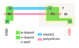
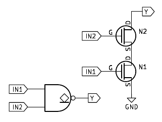
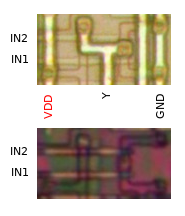
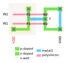
NAND2_A
NAND gate with two inputs.
 |
| I/O | Description |
|---|
| IN1, IN2 |
Inputs to NAND gate. |
| Y |
Outputs !(IN1 && IN2). |
|
Instances:
ZOXC
(1 total)
NAND2_B
NAND gate with two inputs.
 |
| I/O | Description |
|---|
| IN1, IN2 |
Inputs to NAND gate. |
| Y |
Outputs !(IN1 && IN2). |
|
Instances:
ZZOM
(1 total)
NAND2_C
NAND gate with two inputs.
 |
| I/O | Description |
|---|
| IN1, IN2 |
Inputs to NAND gate. |
| Y |
Outputs !(IN1 && IN2). |
|
Instances:
ZAOC
(1 total)
NAND2_D
NAND gate with two inputs.
 |
| I/O | Description |
|---|
| IN1, IN2 |
Inputs to NAND gate. |
| Y |
Outputs !(IN1 && IN2). |
|
Instances:
ZIKS
(1 total)
NAND2_IN1_N_A
NAND gate with two inputs, one of them inverted.
 |
| I/O | Description |
|---|
| IN1 |
Inverted input to NAND gate. |
| IN2 |
Non-inverted input to NAND gate. |
| Y |
Outputs !(!IN1 && IN2). |
|
Instances:
WERF
(1 total)
NAND2_IN1_N_B
NAND gate with two inputs, one of them inverted.
 |
| I/O | Description |
|---|
| IN1 |
Inverted input to NAND gate. |
| IN2 |
Non-inverted input to NAND gate. |
| Y |
Outputs !(!IN1 && IN2). |
|
Instances:
WEEN
(1 total)
NAND2_IN1_N_C
NAND gate with two inputs, one of them inverted.
 |
| I/O | Description |
|---|
| IN1 |
Inverted input to NAND gate. |
| IN2 |
Non-inverted input to NAND gate. |
| Y |
Outputs !(!IN1 && IN2). |
|
Instances:
WUDZ
(1 total)
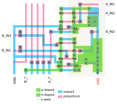
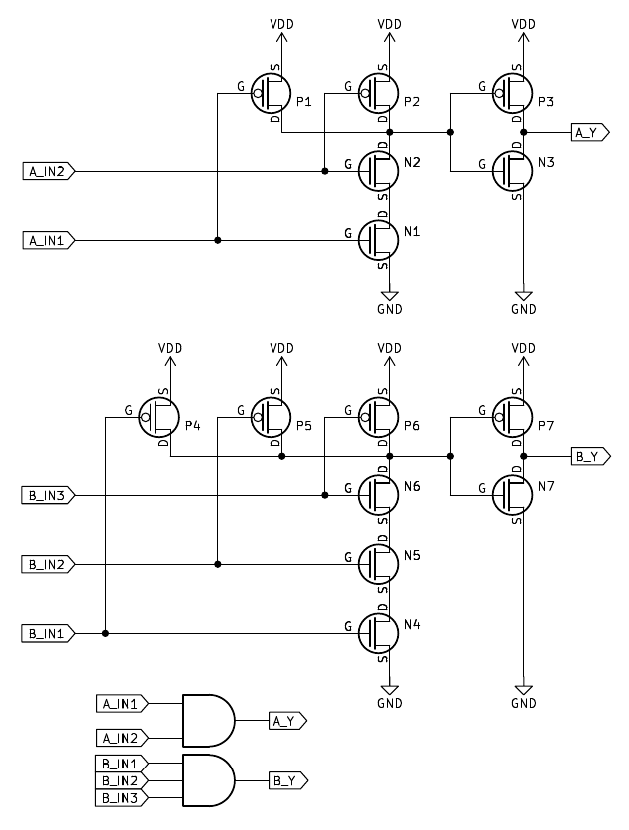
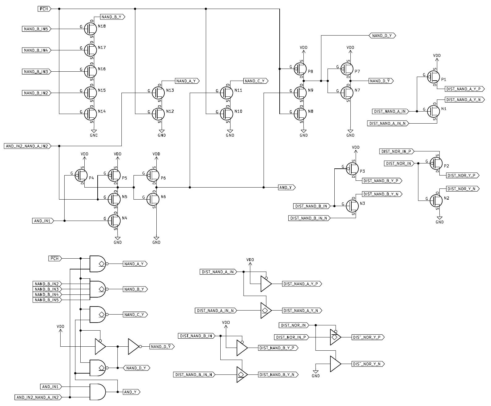
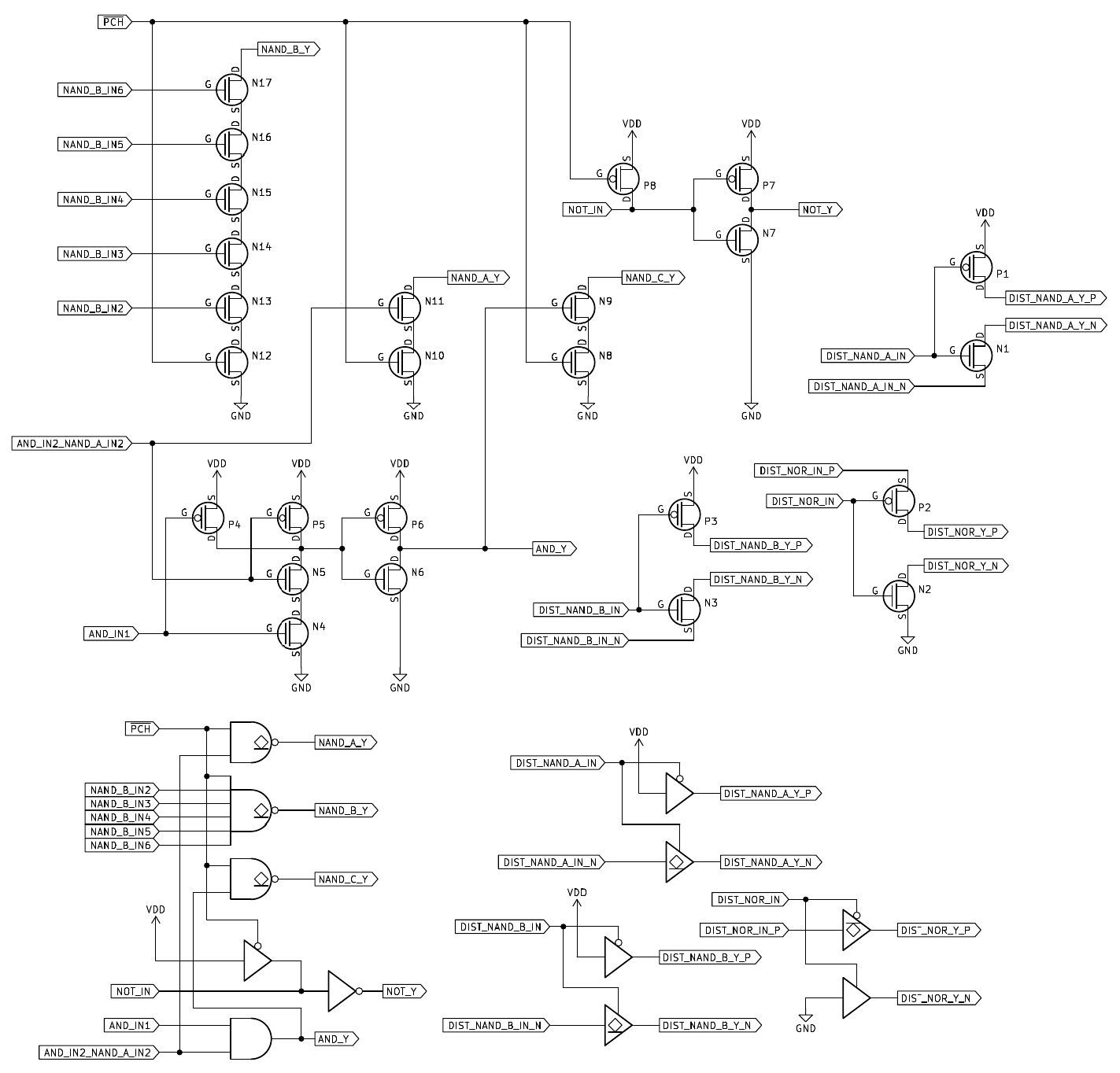
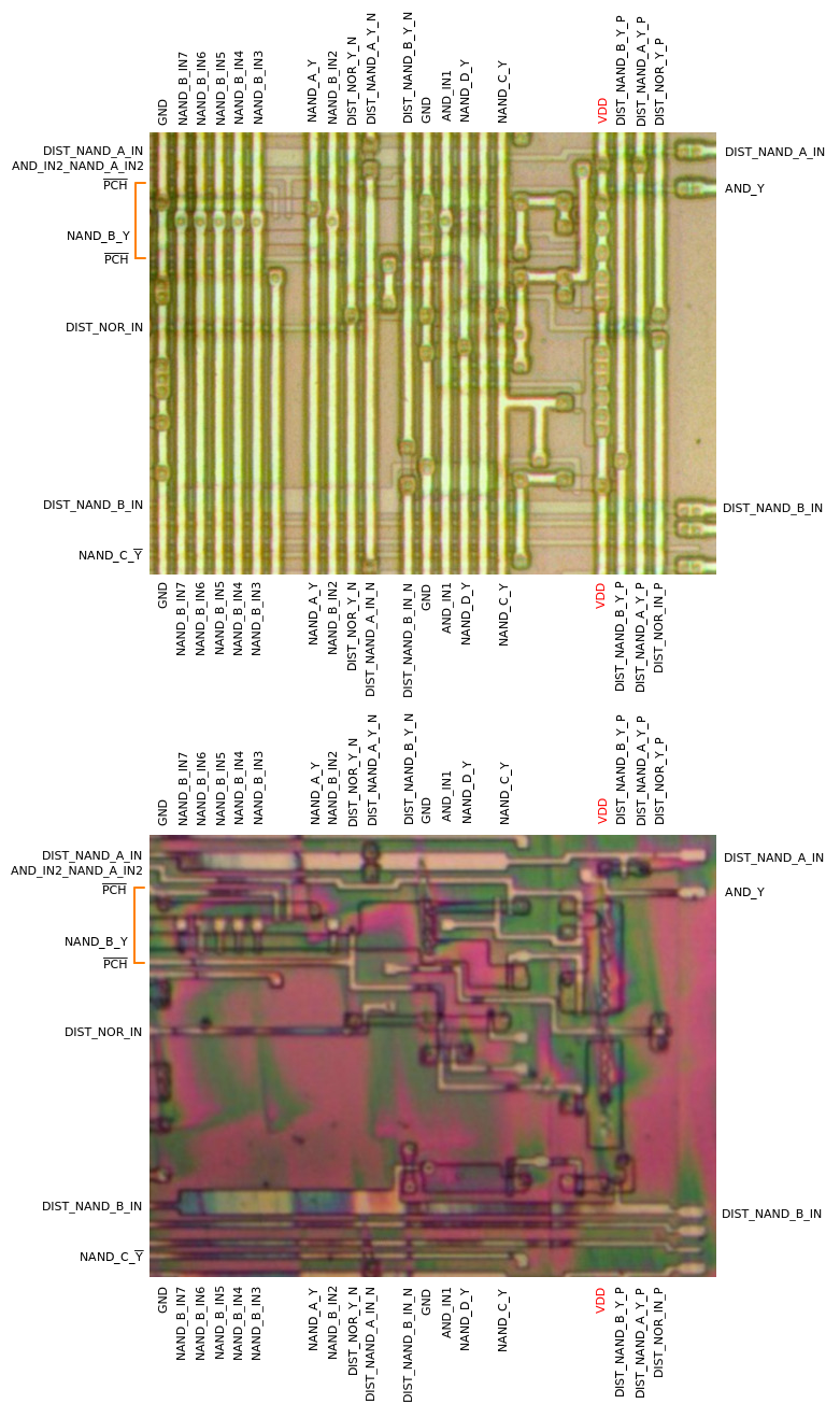
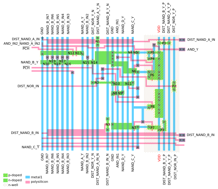
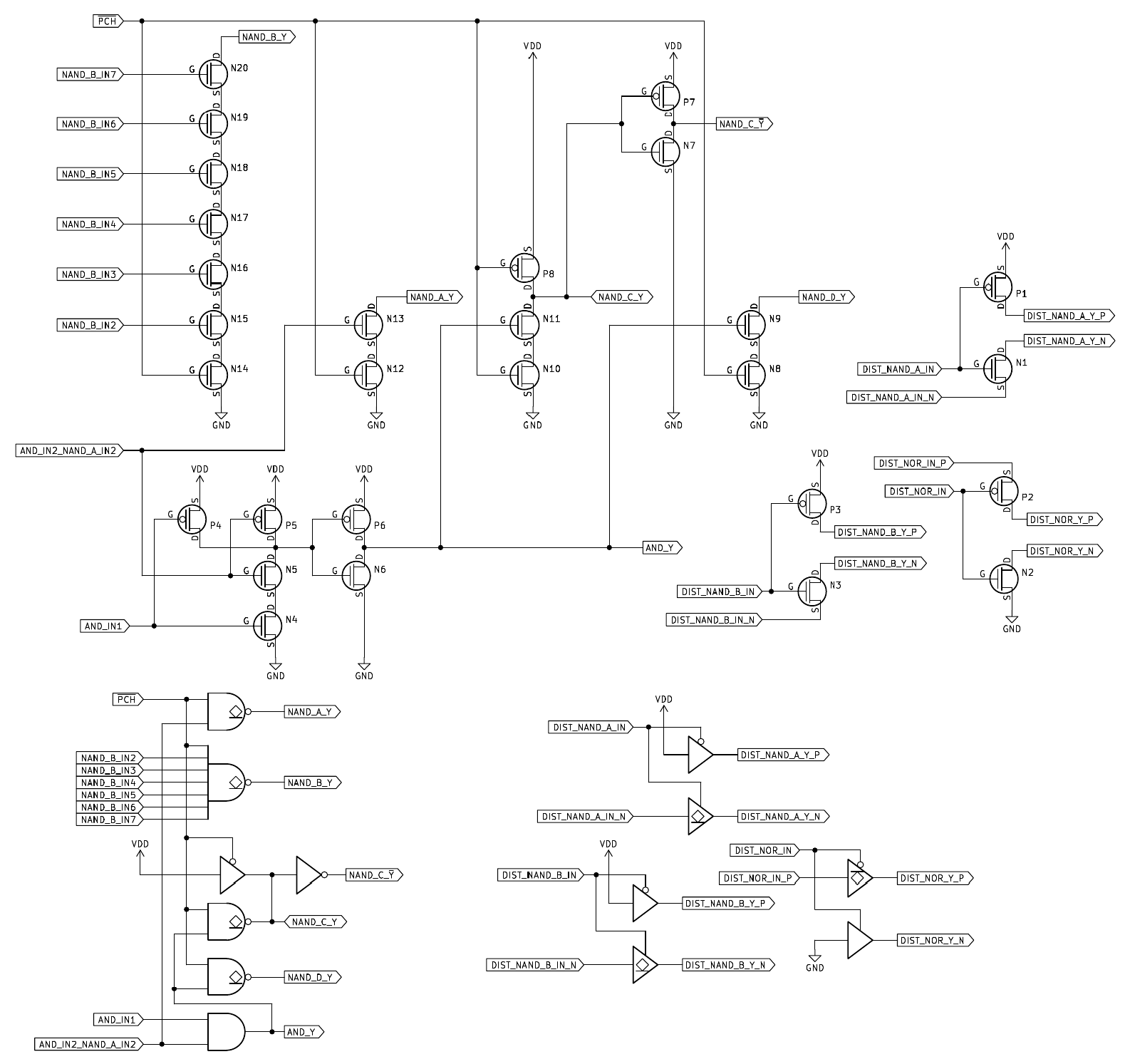
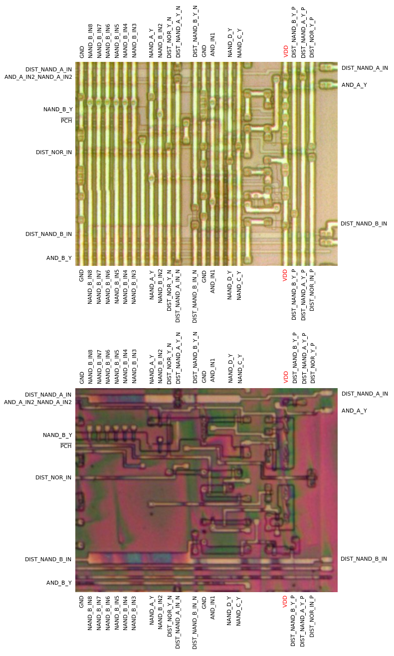
NAND2_NAND3_OD_IRQ
NAND gate with two inputs and open-drain NAND gate with three inputs.
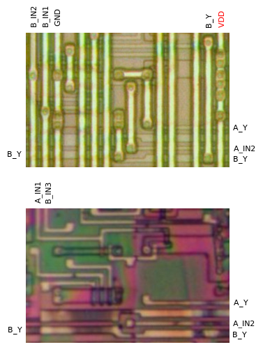 |
| I/O | Description |
|---|
| A_IN1, A_IN2 |
Inputs to NAND gate A. |
| A_Y |
Outputs !(A_IN1 && A_IN2). |
| B_IN1, B_IN2, B_IN3 |
Inputs to NAND gate B. |
| B_Y |
Open-drain output. Outputs !(B_IN1 && B_IN2 && B_IN3). |
|
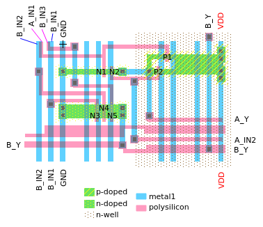
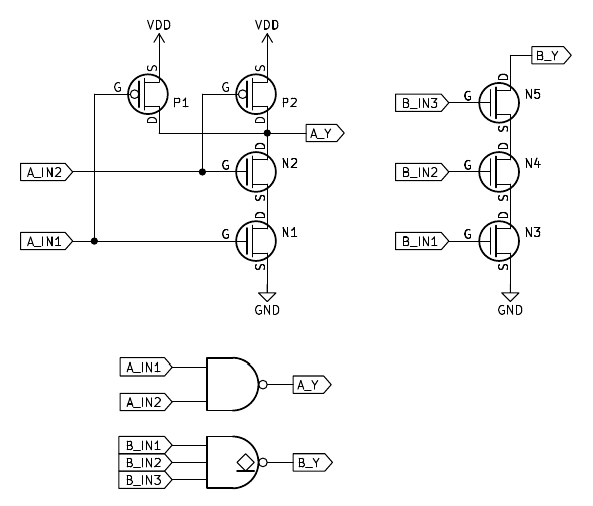
Instances:
IRQ_NAND2_NAND3[0],
IRQ_NAND2_NAND3[1],
IRQ_NAND2_NAND3[2],
IRQ_NAND2_NAND3[3],
IRQ_NAND2_NAND3[4],
IRQ_NAND2_NAND3[5],
IRQ_NAND2_NAND3[6],
IRQ_NAND2_NAND3[7]
(8 total)
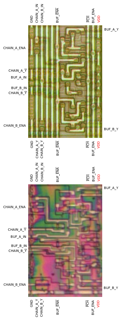
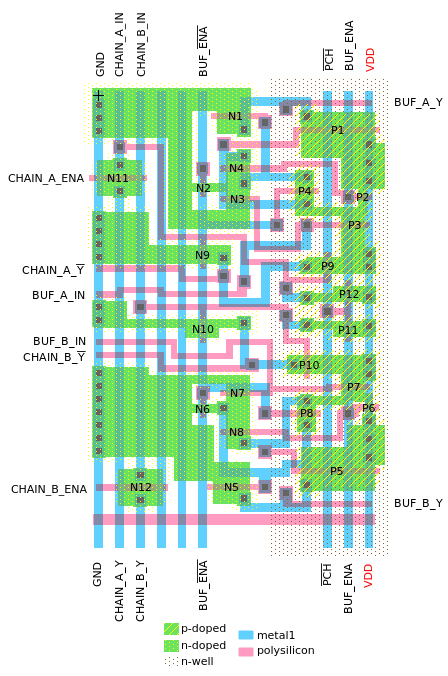
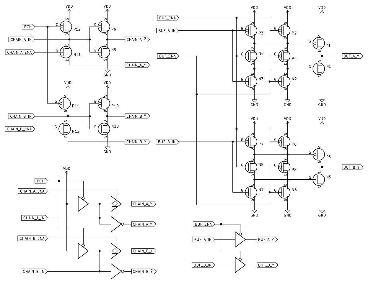
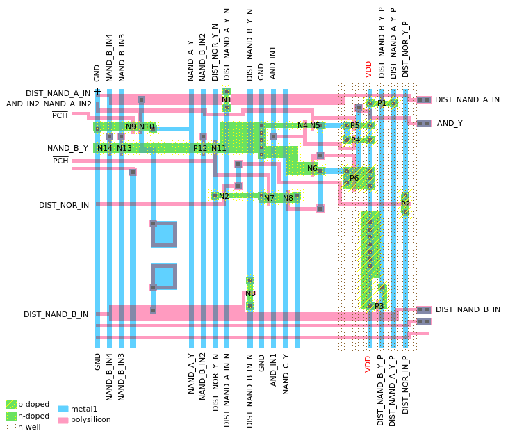
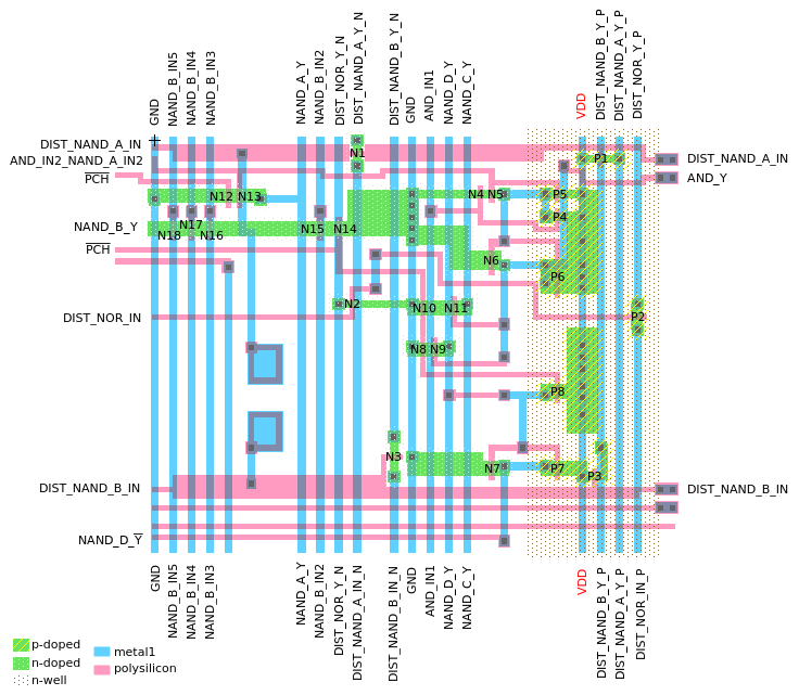
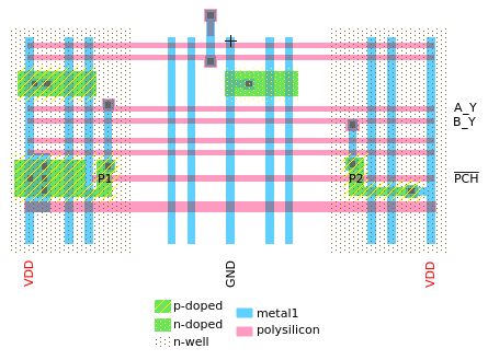
REG_A_OUT
Output drivers for A registers.
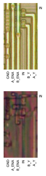 |
| I/O | Description |
|---|
| A_ENA |
Input to NAND gate A. |
| B_ENA |
Input to NAND gate B. |
| IN |
Input to both NAND gates. |
| A_Y |
Open-drain output. Outputs !(A_ENA && IN). |
| B_Y |
Open-drain output. Outputs !(B_ENA && IN). |
|
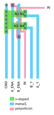
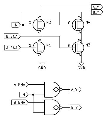
Instances:
REG_A_OUT[0],
REG_A_OUT[1],
REG_A_OUT[2],
REG_A_OUT[3],
REG_A_OUT[4],
REG_A_OUT[5],
REG_A_OUT[6],
REG_A_OUT[7]
(8 total)
NAND2_OD_A_DBUS
Open-drain NAND gate with two inputs.
 |
| I/O | Description |
|---|
| IN1, IN2 |
Inputs to NAND gate. |
| Y |
Open-drain output. Outputs !(IN1 && IN2). |
|
Instances:
DBUS_NAND[0],
DBUS_NAND[2],
DBUS_NAND[4],
DBUS_NAND[6]
(4 total)
NAND2_OD_B_DBUS
Open-drain NAND gate with two inputs.
 |
| I/O | Description |
|---|
| IN1, IN2 |
Inputs to NAND gate. |
| Y |
Open-drain output. Outputs !(IN1 && IN2). |
|
Instances:
DBUS_NAND[1],
DBUS_NAND[3],
DBUS_NAND[5],
DBUS_NAND[7]
(4 total)
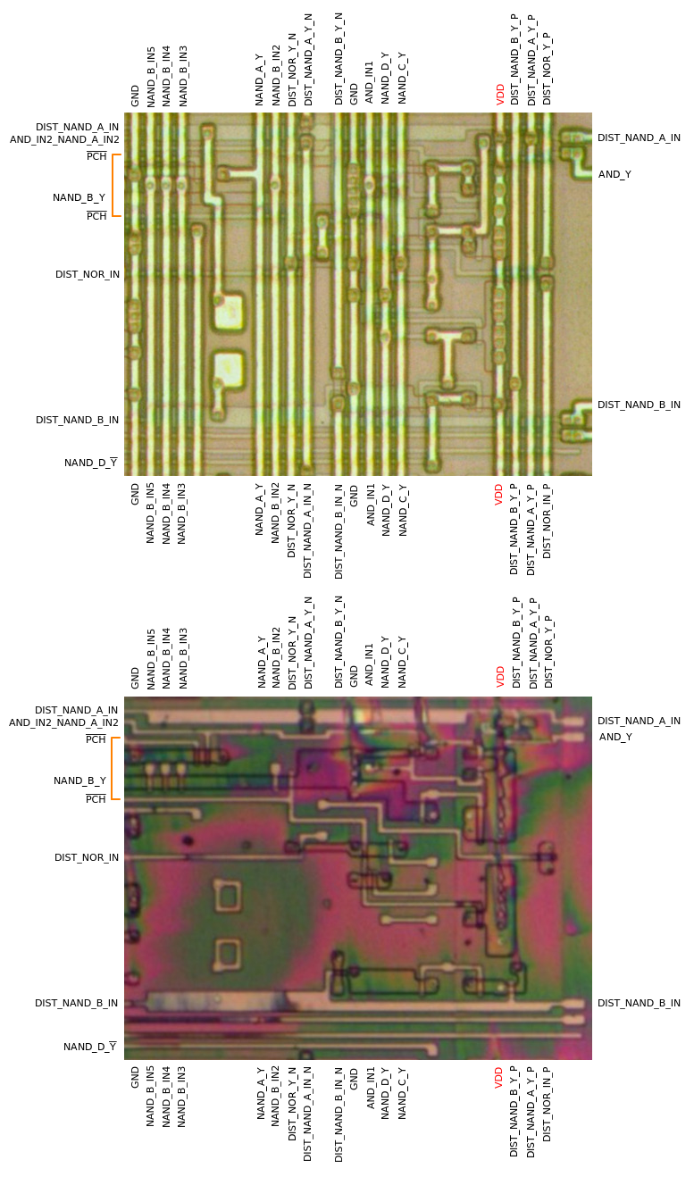
NAND2_SPARE
NAND gate with two inputs.
There is one external connection always made on this cell (see orange line in the picture) that is required
to connect the two Y outputs.
 |
| I/O | Description |
|---|
| IN1, IN2 |
Inputs to NAND gate. |
| Y |
Outputs !(IN1 && IN2). |
|
Instances:
SPARE_NAND
(1 total)
NOR gates
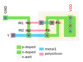
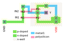
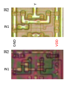
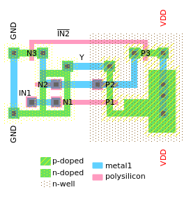
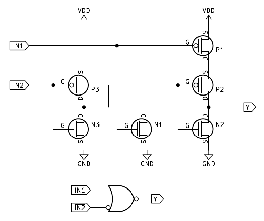
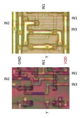
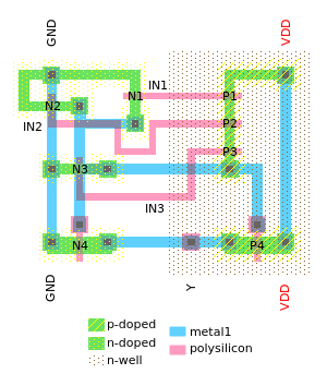
NOR2_A
NOR gate with two inputs.
 |
| I/O | Description |
|---|
| IN1, IN2 |
Inputs to NOR gate. |
| Y |
Outputs !(IN1 || IN2). |
|
Instances:
ZOWA
(1 total)
NOR2_B
NOR gate with two inputs.
 |
| I/O | Description |
|---|
| IN1, IN2 |
Inputs to NOR gate. |
| Y |
Outputs !(IN1 || IN2). |
|
Instances:
ZWLM
(1 total)
NOR2_C
NOR gate with two inputs.
 |
| I/O | Description |
|---|
| IN1, IN2 |
Inputs to NOR gate. |
| Y |
Outputs !(IN1 || IN2). |
|
Instances:
YNIU
(1 total)
NOR2_D
NOR gate with two inputs.
 |
| I/O | Description |
|---|
| IN1, IN2 |
Inputs to NOR gate. |
| Y |
Outputs !(IN1 || IN2). |
|
Instances:
WAGR
(1 total)
NOR2_E
NOR gate with two inputs.
 |
| I/O | Description |
|---|
| IN1, IN2 |
Inputs to NOR gate. |
| Y |
Outputs !(IN1 || IN2). |
|
Instances:
WAFR
(1 total)
NOR2_F
NOR gate with two inputs.
 |
| I/O | Description |
|---|
| IN1, IN2 |
Inputs to NOR gate. |
| Y |
Outputs !(IN1 || IN2). |
|
Instances:
ZHZO
(1 total)
NOR3
NOR gate with three inputs.
 |
| I/O | Description |
|---|
| IN1, IN2, IN3 |
Inputs to NOR gate. |
| Y |
Outputs !(IN1 || IN2 || IN3). |
|
Instances:
XYGB
(1 total)
NOR2_IN2_N
NOR gate with two inputs, one of them inverted.
 |
| I/O | Description |
|---|
| IN1 |
Non-inverted input to NOR gate. |
| IN2 |
Inverted input to NOR gate. |
| Y |
Outputs !(IN1 || !IN2). |
|
Instances:
YOLU
(1 total)
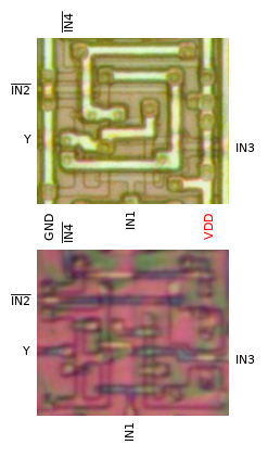
NOR4_IN2_N_IN4_N
NOR gate with four inputs, two of them inverted.
 |
| I/O | Description |
|---|
| IN1, IN3 |
Non-inverted inputs to NOR gate. |
| IN2,
IN4 |
Inverted inputs to NOR gate. |
| Y |
Outputs !(IN1 || !IN2 || IN3 || !IN4). |
|
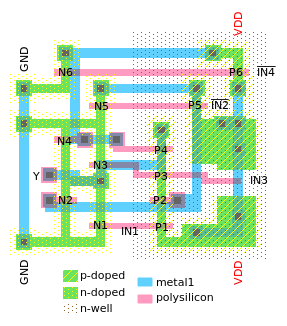
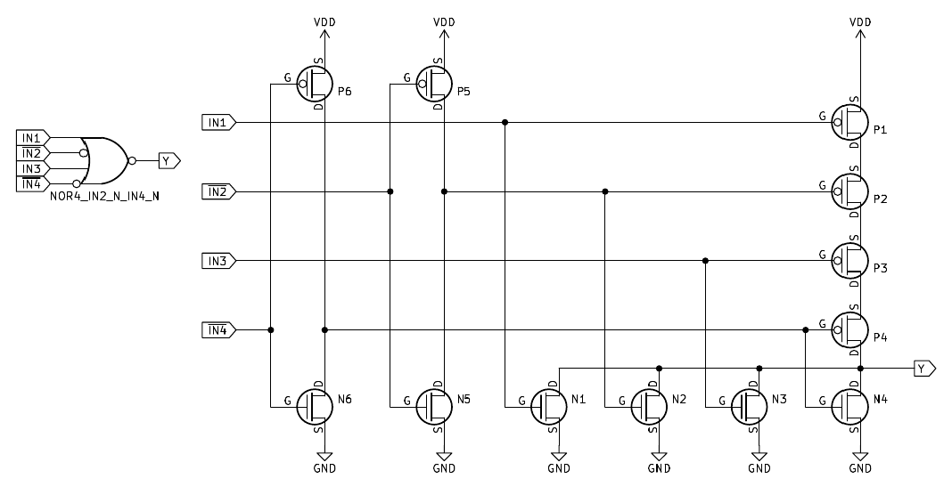
Instances:
ZAIJ
(1 total)
NOR2_PCH_IN1_DEC3
NOR gate with two inputs and precharge on input 1.
 |
| I/O | Description |
|---|
| IN1 |
Input to NOR gate. Outputs high if PCH is low. |
| IN2 |
Input to NOR gate. |
| Y |
Outputs !(IN1 || IN2). |
| PCH |
Active-low precharge input. If low, IN1 gets driven high for the purpose of precharging the net
connected to the input. |
|
Instances:
DEC3_NOR1,
DEC3_NOR2
(2 total)
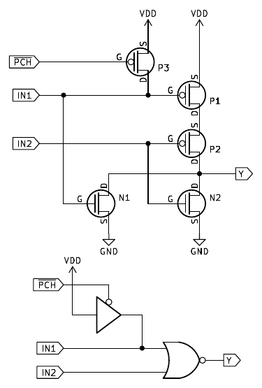
NOR8_ALU
NOR gate with eight inputs.
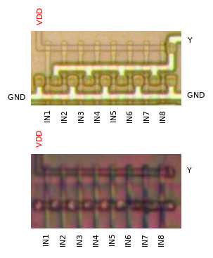 |
| I/O | Description |
|---|
| IN1, IN2, IN3, IN4, IN5, IN6, IN7, IN8 |
Inputs to NOR gate. |
| Y |
Outputs !(IN1 || IN2 || IN3 || IN4 || IN5 || IN6 || IN7 || IN8). |
|
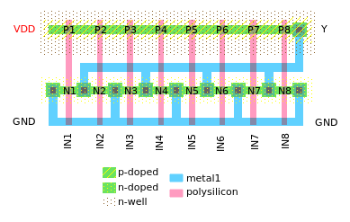
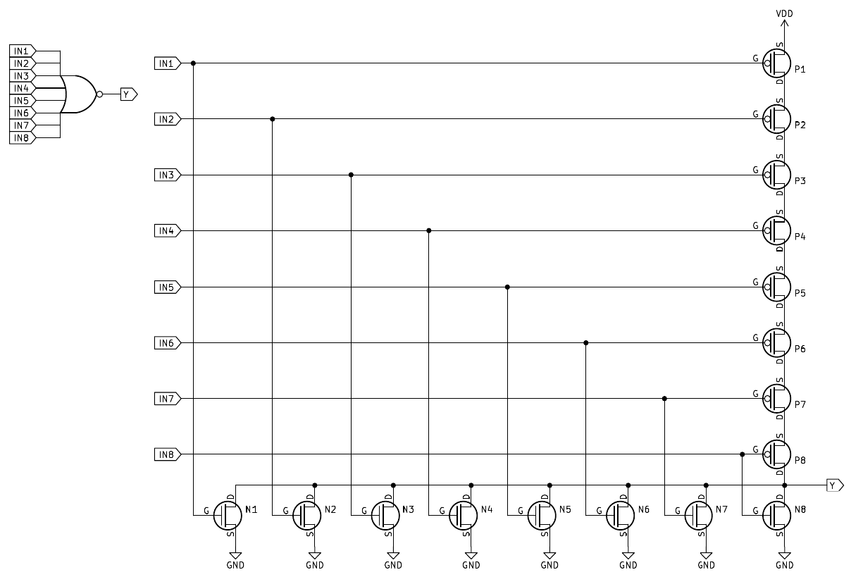
Instances:
ALU_ZGEN
(1 total)
NOR2_SPARE
NOR gate with two inputs.
 |
| I/O | Description |
|---|
| IN1, IN2 |
Inputs to NOR gate. |
| Y |
Outputs !(IN1 || IN2). |
|
Instances:
SPARE_NOR
(1 total)
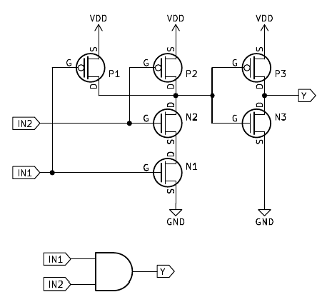
AND gates
AND2
AND gate with two inputs.
 |
| I/O | Description |
|---|
| IN1, IN2 |
Inputs to AND gate. |
| Y |
Outputs (IN1 && IN2). |
|
Instances:
ZIUL
(1 total)
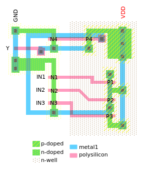
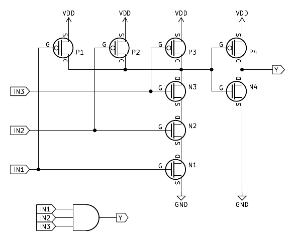
AND3
AND gate with three inputs.
 |
| I/O | Description |
|---|
| IN1, IN2, IN3 |
Inputs to AND gate. |
| Y |
Outputs (IN1 && IN2 && IN3). |
|
Instances:
ZYOC
(1 total)
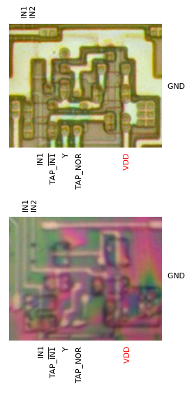
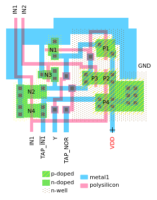
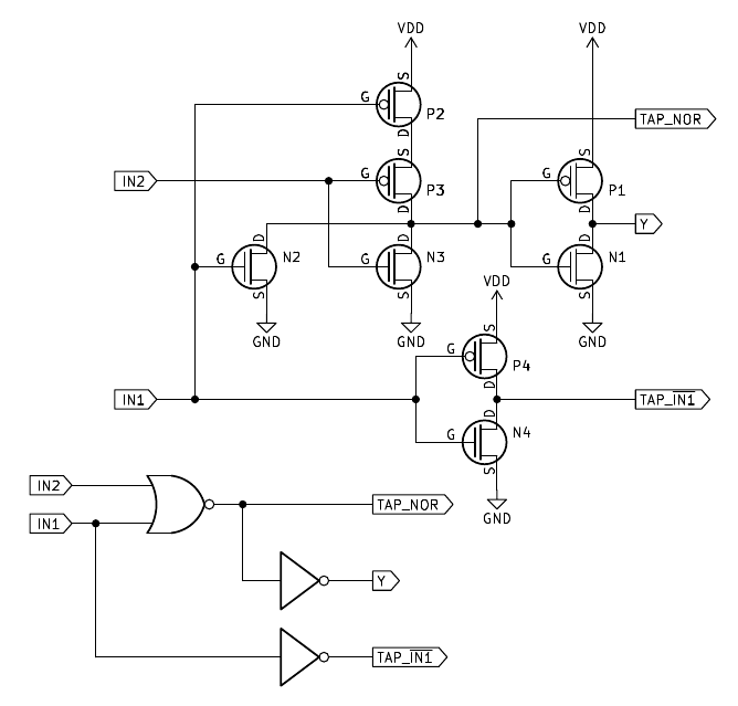
AND2_IN1_N_TAP_IN1
AND gate with two inputs, inverted first input, and tap after inversion of first input.
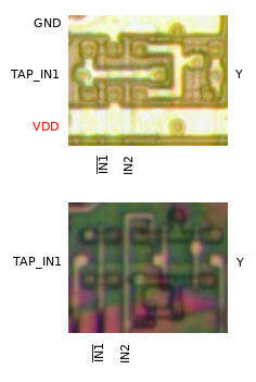 |
| I/O | Description |
|---|
| IN1 |
Inverted input to AND gate. |
| IN2 |
Non-inverted input to AND gate. |
| Y |
Outputs (!IN1 && IN2). |
| TAP_IN1 |
Outputs inverted IN1. |
|
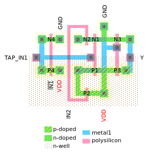
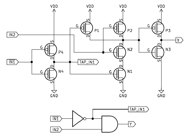
Instances:
VEQU
(1 total)
AND2_IRQ
AND gate with two inputs.
 |
| I/O | Description |
|---|
| IN1, IN2 |
Inputs to AND gate. |
| Y |
Outputs (IN1 && IN2). |
|
Instances:
IRQ_AND
(1 total)
AND2_REG
AND gate with two inputs.
 |
| I/O | Description |
|---|
| IN1, IN2 |
Inputs to AND gate. |
| Y |
Outputs (IN1 && IN2). |
|
Instances:
REG_AND
(1 total)
AND2_AND3_REG
Group of two AND gates with two and three inputs.
 |
| I/O | Description |
|---|
| A_IN1, A_IN2 |
Inputs to AND gate A. |
| A_Y |
Outputs (A_IN1 && A_IN2). |
| B_IN1, B_IN2, B_IN3 |
Inputs to AND gate B. |
| B_Y |
Outputs (B_IN1 && B_IN2 && B_IN3). |
|
Instances:
REG_AND2_AND3
(1 total)
AND2_ALU
AND gate with two inputs.
 |
| I/O | Description |
|---|
| IN1, IN2 |
Inputs to AND gate. |
| Y |
Outputs (IN1 && IN2). |
|
Instances:
ALU_AND[0],
ALU_AND[1],
ALU_AND[2],
ALU_AND[3],
ALU_AND[4],
ALU_AND[5],
ALU_AND[6],
ALU_AND[7]
(8 total)
OR gates
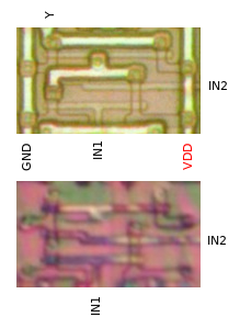
OR2_A
OR gate with two inputs.
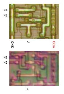 |
| I/O | Description |
|---|
| IN1, IN2 |
Inputs to OR gate. |
| Y |
Outputs (IN1 || IN2). |
|
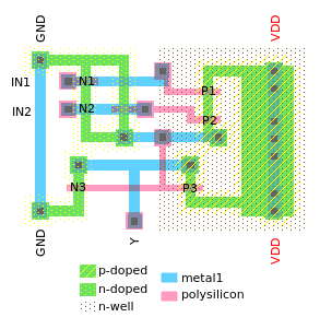
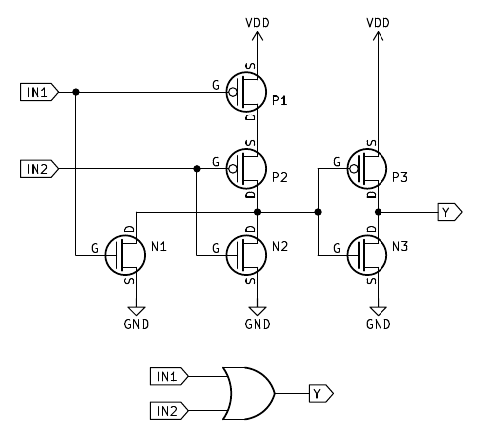
Instances:
ZNDA
(1 total)
OR2_B
OR gate with two inputs.
 |
| I/O | Description |
|---|
| IN1, IN2 |
Inputs to OR gate. |
| Y |
Outputs (IN1 || IN2). |
|
Instances:
ZFEX
(1 total)
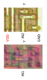
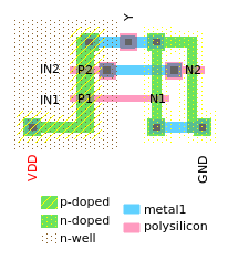
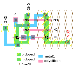
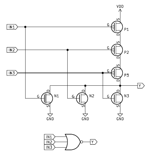
OR3_A
OR gate with three inputs.
 |
| I/O | Description |
|---|
| IN1, IN2, IN3 |
Inputs to OR gate. |
| Y |
Outputs (IN1 || IN2 || IN3). |
|
Instances:
YNOZ
(1 total)
OR3_B
OR gate with three inputs.
 |
| I/O | Description |
|---|
| IN1, IN2, IN3 |
Inputs to OR gate. |
| Y |
Outputs (IN1 || IN2 || IN3). |
|
Instances:
YCNF
(1 total)
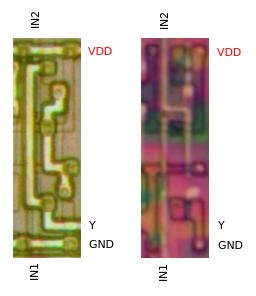
OR2_TAP_NOR_TAP_IN1_N_REG
OR gate with two inputs, tap on intermediate NOR, and inverting tap on IN1.
 |
| I/O | Description |
|---|
| IN1 |
Input to OR gate and inverter. |
| IN2 |
Input to OR gate. |
| Y |
Outputs (IN1 || IN2). |
| TAP_NOR |
Outputs !(IN1 || IN2). |
| TAP_IN1 |
Outputs inverted IN1. |
|
Instances:
REG_OR
(1 total)
XOR gates
XOR_IDU_H
XOR gate with two inputs.
There is one external connection always made on this cell (see orange line in the picture) that is required
to connect the two IN1 inputs.
 |
| I/O | Description |
|---|
| IN1, IN2 |
Inputs to XOR gate. There are two IN1 inputs to this cell, which are externally connected to each other
(indicated by the orange line in the picture). |
| Y |
Outputs (IN1 ^ IN2). |
|
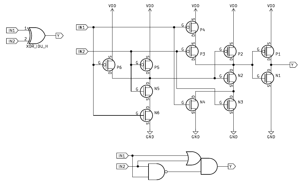
Instances:
IDU_XOR_H[0],
IDU_XOR_H[1],
IDU_XOR_H[2],
IDU_XOR_H[3],
IDU_XOR_H[4],
IDU_XOR_H[5],
IDU_XOR_H[6],
IDU_XOR_H[7]
(8 total)
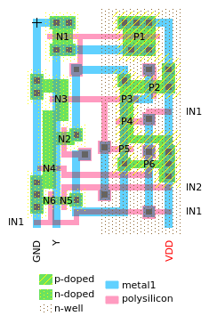
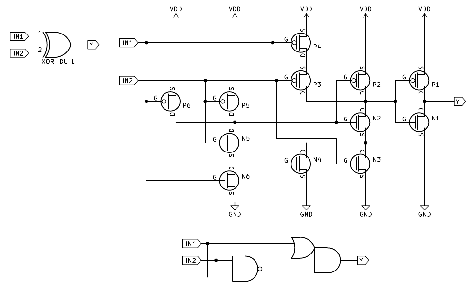
XOR_IDU_L
XOR gate with two inputs.
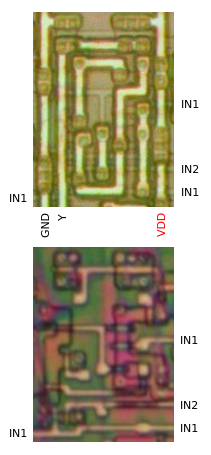 |
| I/O | Description |
|---|
| IN1, IN2 |
Inputs to XOR gate. |
| Y |
Outputs (IN1 ^ IN2). |
|
Instances:
IDU_XOR_L[0],
IDU_XOR_L[1],
IDU_XOR_L[2],
IDU_XOR_L[3],
IDU_XOR_L[4],
IDU_XOR_L[5],
IDU_XOR_L[6],
IDU_XOR_L[7]
(8 total)
Compound logic gates
AOI21_A
2-1 AND-OR-INVERT two-level compound gate.
 |
| I/O | Description |
|---|
| IN1, IN2 |
Inputs to AND gate. |
| IN3 |
Input to OR gate. |
| Y |
Outputs !((IN1 && IN2) || IN3). |
|
Instances:
YNEU
(1 total)
AOI21_B
2-1 AND-OR-INVERT two-level compound gate.
 |
| I/O | Description |
|---|
| IN1, IN2 |
Inputs to AND gate. |
| IN3 |
Input to OR gate. |
| Y |
Outputs !((IN1 && IN2) || IN3). |
|
Instances:
XTIP
(1 total)
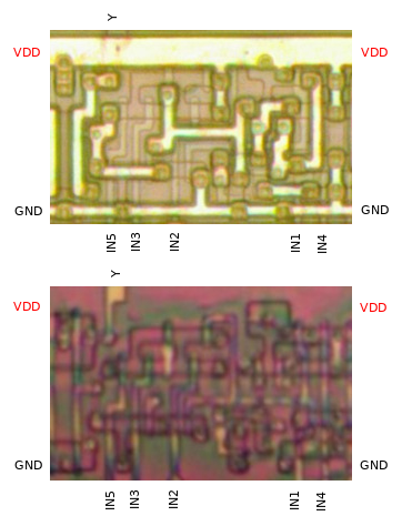
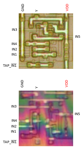
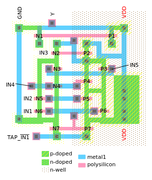
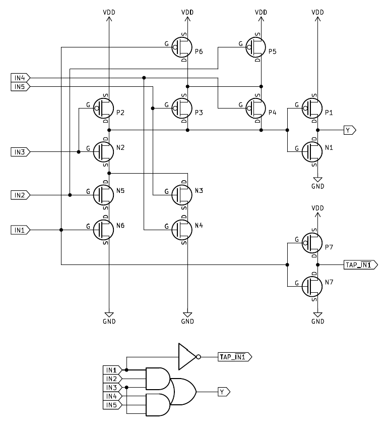
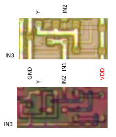
AOI331_S3
3-3-1 AND-OR-INVERT two-level compound gate with shared IN3.
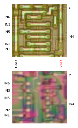 |
| I/O | Description |
|---|
| IN1, IN2, IN3, IN4, IN5 |
Inputs to AND gates. |
| IN6 |
Input to OR gate. |
| Y |
Outputs !((IN1 && IN2 && IN3) || (IN4 && IN5 && IN3) || IN6). |
|
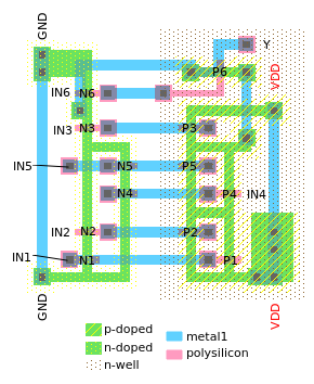
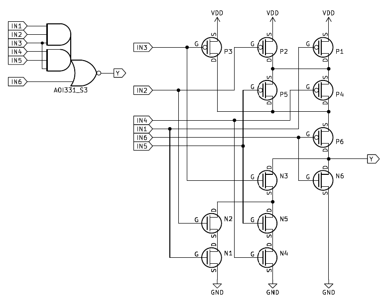
Instances:
ZWUU
(1 total)
AO221_XOR_IN4_S1
2-2-1 AND-OR two-level compound gate with XOR gate feeding IN4, and shared IN1 between both gates. The XOR gate
in this cell functions as the sum generator of the carry lookahead adder (CLA).
 |
| I/O | Description |
|---|
| IN1 |
Shared input to XOR gate and first AND gate. |
| IN2, IN3 |
Inputs to AND gates. |
| IN4 |
Input to XOR gate. |
| IN5 |
Input to OR gate. |
| Y |
Outputs ((IN1 && IN2) || (IN3 && (IN1 ^ IN4)) || IN5). |
|
Instances:
ALU_RESULT[0],
ALU_RESULT[1],
ALU_RESULT[2],
ALU_RESULT[3],
ALU_RESULT[4],
ALU_RESULT[5],
ALU_RESULT[6],
ALU_RESULT[7]
(8 total)
AO31_IN3_N
3-1 AND-OR two-level compound gate with inverted third input.
 |
| I/O | Description |
|---|
| IN1, IN2 |
Non-inverted inputs to AND gate. |
| IN3 |
Inverted input to AND gate. |
| IN4 |
Input to OR gate. |
| Y |
Outputs ((IN1 && IN2 && !IN3) || IN4). |
|

Instances:
XOGS
(1 total)
AO33_S3_TAP_IN1_N
3-3 AND-OR two-level compound gate with shared IN3, and inverting tap on IN1.
 |
| I/O | Description |
|---|
| IN1, IN2, IN3, IN4, IN5 |
Inputs to AND gates. |
| Y |
Outputs ((IN1 && IN2 && IN3) || (IN4 && IN5 && IN3)). |
| TAP_IN1 |
Outputs inverted IN1. |
|
Instances:
ZBPP
(1 total)
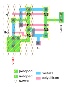
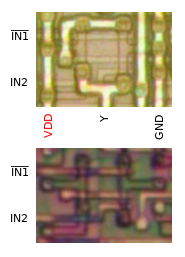
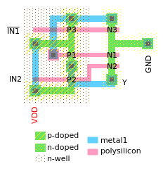
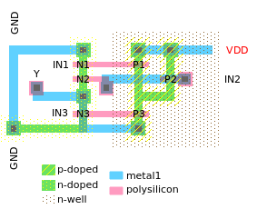
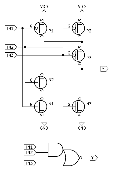
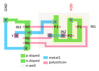
OAI21
2-1 OR-AND-INVERT two-level compound gate.
 |
| I/O | Description |
|---|
| IN1, IN2 |
Inputs to OR gate. |
| IN3 |
Input to AND gate. |
| Y |
Outputs !((IN1 || IN2) && IN3). |
|
Instances:
YKUA
(1 total)
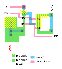
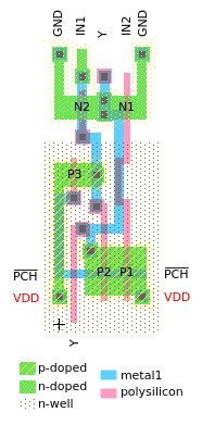
OA21
2-1 OR-AND two-level compound gate.
 |
| I/O | Description |
|---|
| IN1, IN2 |
Inputs to OR gate. |
| IN3 |
Input to AND gate. |
| Y |
Outputs ((IN1 || IN2) && IN3). |
|
Instances:
WDIN
(1 total)
OA21_REG
2-1 OR-AND two-level compound gate.
 |
| I/O | Description |
|---|
| IN1, IN2 |
Inputs to OR gate. |
| IN3 |
Input to AND gate. |
| Y |
Outputs ((IN1 || IN2) && IN3). |
|
Instances:
REG_OA1,
REG_OA2
(2 total)
OA211_IN1_N_IN3_N
2-1-1 OR-AND two-level compound gate with inverted IN1 and IN3.
 |
| I/O | Description |
|---|
| IN1 |
Inverted input to OR gate. |
| IN2 |
Non-inverted input to OR gate. |
| IN3 |
Inverted input to AND gate. |
| IN4 |
Non-inverted input to AND gate. |
| Y |
Outputs ((!IN1 || IN2) && !IN3 && IN4). |
|
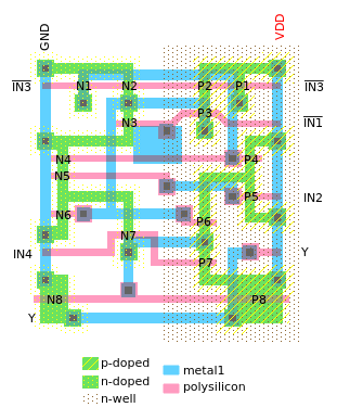
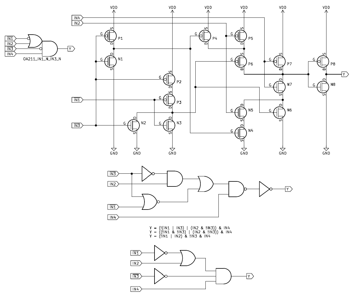
Instances:
ZLYZ
(1 total)
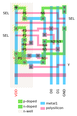
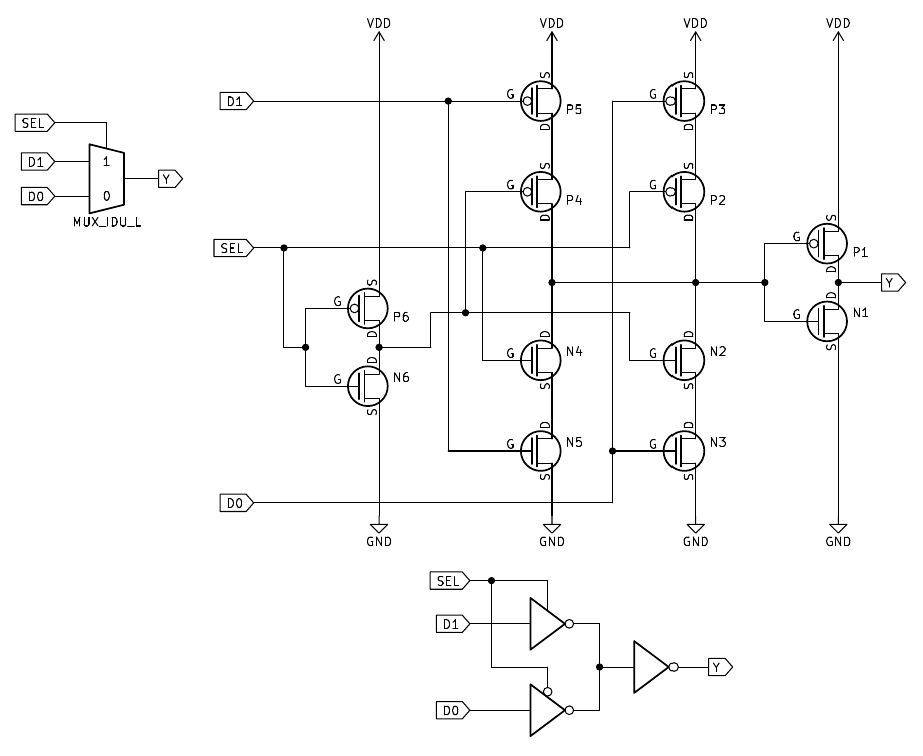
MUX_IDU_H
Multiplexer with two inputs.
There is one external connection always made on this cell (see orange line in the picture) that is required
to connect the two SEL inputs.
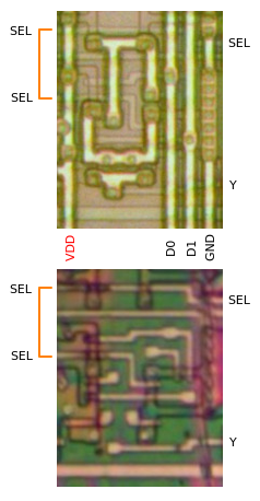 |
| I/O | Description |
|---|
| D0, D1 |
Data inputs. |
| SEL |
Select input. There are two SEL inputs to this cell, which are externally connected to each other
(indicated by the orange line in the picture). |
| Y |
Outputs D1 if SEL is high; outputs D0
if SEL is low. |
|
Instances:
IDU_MUX_H[0],
IDU_MUX_H[1],
IDU_MUX_H[2],
IDU_MUX_H[3],
IDU_MUX_H[4],
IDU_MUX_H[5],
IDU_MUX_H[6],
IDU_MUX_H[7]
(8 total)
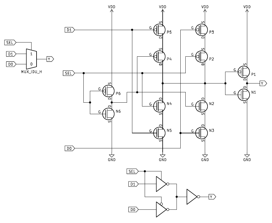
MUX_IDU_L
Multiplexer with two inputs.
There is one external connection always made on this cell (see orange line in the picture) that is required
to connect the two SEL inputs.
 |
| I/O | Description |
|---|
| D0, D1 |
Data inputs. |
| SEL |
Select input. There are two SEL inputs to this cell, which are externally connected to each other
(indicated by the orange line in the picture). |
| Y |
Outputs D1 if SEL is high; outputs D0
if SEL is low. |
|
Instances:
IDU_MUX_L[0],
IDU_MUX_L[1],
IDU_MUX_L[2],
IDU_MUX_L[3],
IDU_MUX_L[4],
IDU_MUX_L[5],
IDU_MUX_L[6],
IDU_MUX_L[7]
(8 total)
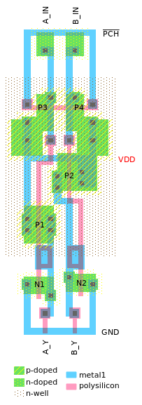
Mixed logic cells
ALU_CGEN
Logic for generating carry signals for the CLA (carry lookahead adder).
The Pn and Gn inputs each consist of two ports that must be externally connected.
This cell must be fed with valid P/G (propagate/generate) signals, otherwise it can short circuit internally,
because the NMOS and PMOS networks are not complementary. The signals are valid if
Pn = An || Bn, and Gn = An && Bn;
when An and Bn are the two operands of a sum operation.
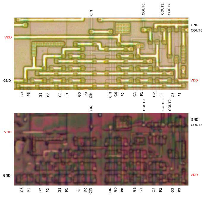 |
| I/O | Description |
|---|
| P0, P1, P2, P3 |
Inputs for propagate signals. |
| G0, G1, G2, G3 |
Inputs for generate signals. |
| CIN |
Input carry signal. |
| COUT0, COUT1, COUT2, COUT3 |
Output carry signals. |
|
Instances:
ALU_CGEN_L,
ALU_CGEN_H
(2 total)
ALU_PGGEN
Logic for generating P/G (propagate/generate) signals for the CLA (carry lookahead adder).
This cell contains a lot of other logic. The P/G signals are just two tap outputs.
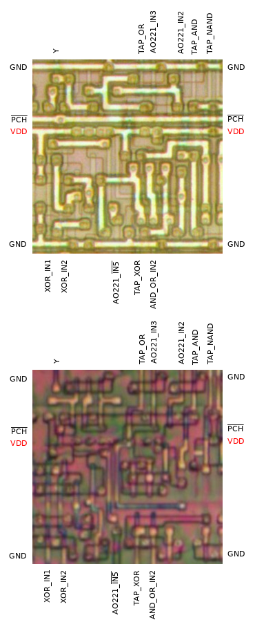 |
| I/O | Description |
|---|
| XOR_IN1, XOR_IN2 |
Inputs to XOR gate. |
| AND_OR_IN2 |
Shared second input for (N)AND and OR gates. |
| AO221_IN2, AO221_IN3 |
Inputs to AND gates of AO221 compound gate. |
| PCH |
Active-low precharge input. If PCH is low then
AO221_IN5 is driven high for the purpose of precharging the
net at the input. |
| AO221_IN5 |
Input to OR gate of AO221 compound gate. Outputs high if PCH
is low. |
| TAP_XOR |
Outputs (XOR_IN1 ^ XOR_IN2). |
| TAP_NAND |
Outputs !((XOR_IN1 ^ XOR_IN2) && AND_OR_IN2). |
| TAP_AND |
Outputs ((XOR_IN1 ^ XOR_IN2) && AND_OR_IN2). This output is used as
generate signal for carry generation. |
| TAP_OR |
Outputs ((XOR_IN1 ^ XOR_IN2) || AND_OR_IN2). This output is used as propagate
signal for carry generation. |
| Y |
Outputs ((TAP_AND && AO221_IN2) || (AO221_IN3 && TAP_OR) || !AO221_IN5). |
|
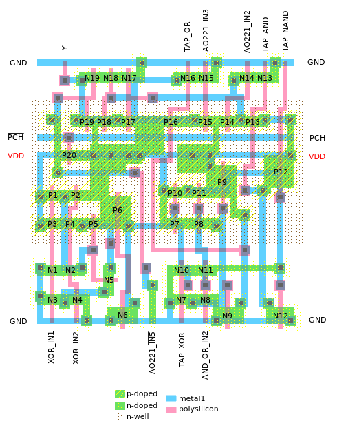
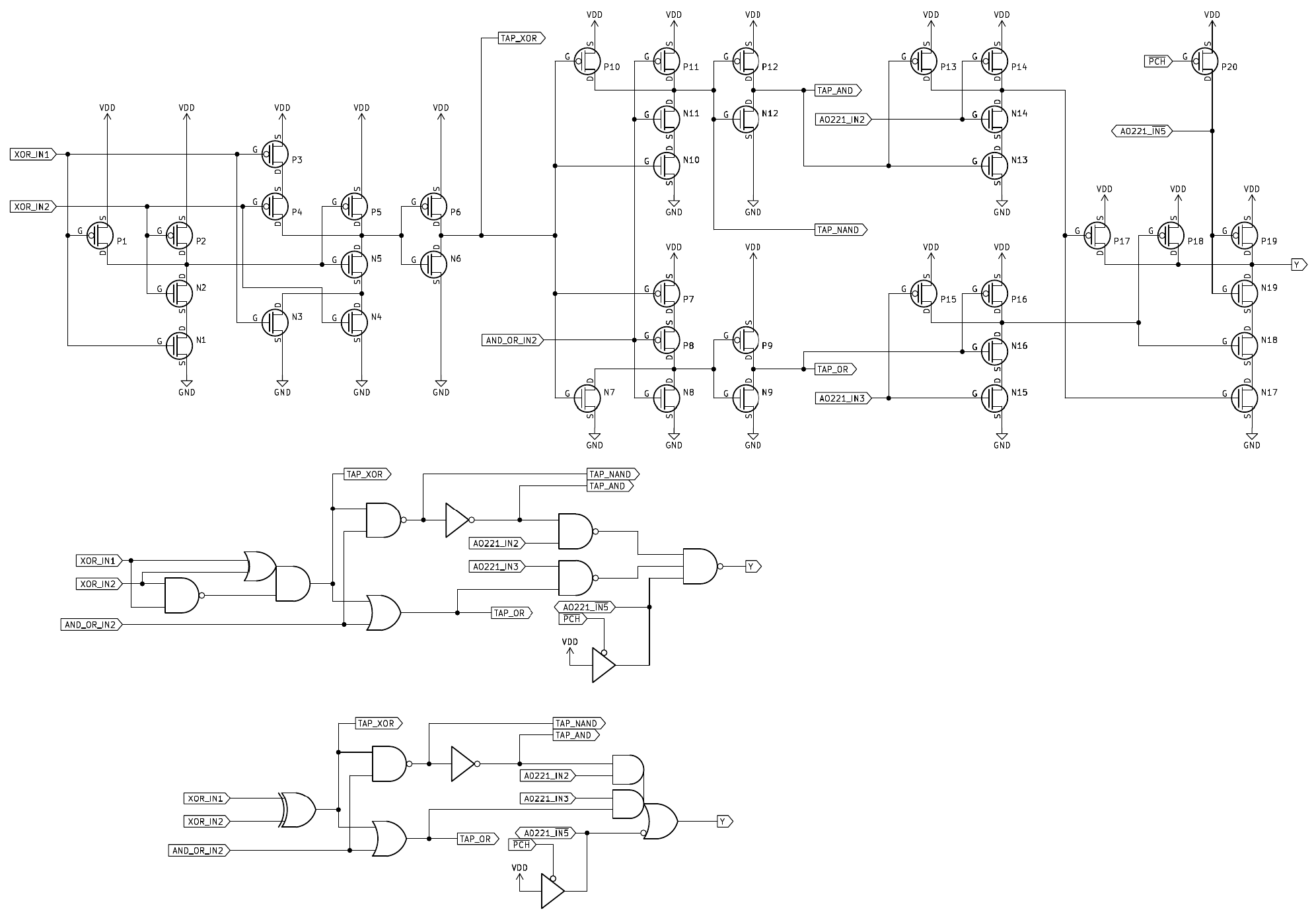
Instances:
ALU_PGGEN[0],
ALU_PGGEN[1],
ALU_PGGEN[2],
ALU_PGGEN[3],
ALU_PGGEN[4],
ALU_PGGEN[5],
ALU_PGGEN[6],
ALU_PGGEN[7]
(8 total)
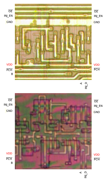
B2B_WAND_INJ_A
Bidirectional bus bridge with wired-AND behavior (open-drain), active-low output enable, active-low
precharge, and open-drain injector on side A.
 |
| I/O | Description |
|---|
| A |
Bidirectional port to bus A. If PCH is high and
INJ_EN is low, then A is driven high. If OE
and B are both low and PCH is high, then A
is driven low. If INJ_EN and PCH are both high and
INJ_D is low, then A is driven low. |
| B |
Bidirectional port to bus B. If PCH is high and
OE is low, then B is driven high. If OE
and A are both low and PCH is high, then B
is driven low. |
| OE |
Active-low bridge enable input. If OE is low and
PCH is high, then a low state on any of the two ports
A or B will cause both ports A and B to be actively driven low until
OE gets released. |
| PCH |
Active-low precharge input. If PCH is low and
OE is high, then port A is driven high. If
PCH and
OE both are low, then both ports A and B
are driven high. INJ_EN must be low while PCH
is low, otherwise the PMOS and NMOS drivers on port A will short circuit. |
| INJ_D |
Injector data input. If INJ_D is low and INJ_EN is high, then port A is driven
low. |
| INJ_EN |
Active-high injector enable input. If INJ_EN is high and INJ_D is low, then port A
is driven low. PCH must be high while INJ_EN is
high, otherwise the PMOS and NMOS drivers on port A will short circuit. |
|
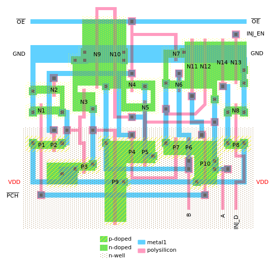
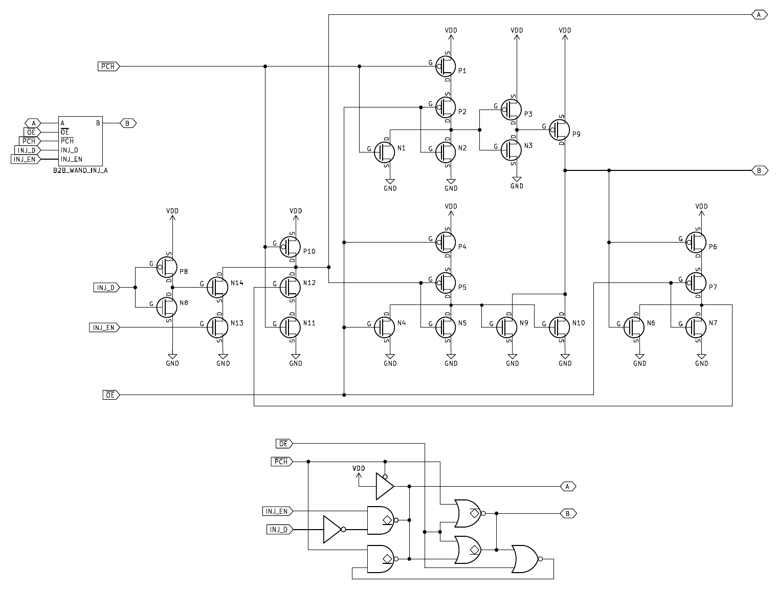
Instances:
DBUS_BRIDGE[0],
DBUS_BRIDGE[1],
DBUS_BRIDGE[2],
DBUS_BRIDGE[3],
DBUS_BRIDGE[4],
DBUS_BRIDGE[5],
DBUS_BRIDGE[6],
DBUS_BRIDGE[7]
(8 total)
IDU_BIT0
Bits 0 and 8 of the 16 bit increment/decrement unit.
 |
| I/O | Description |
|---|
| |
TODO: Describe I/Os |
|
Instances:
IDU[0]
(1 total)
IDU_BIT123456
Bits 1-6 and 9-14 of the 16 bit increment/decrement unit.
 |
| I/O | Description |
|---|
| |
TODO: Describe I/Os |
|
Instances:
IDU[1]
IDU[2]
IDU[3]
IDU[4]
IDU[5]
IDU[6]
(6 total)
IDU_BIT7
Bits 7 and 15 of the 16 bit increment/decrement unit.
 |
| I/O | Description |
|---|
| |
TODO: Describe I/Os |
|
Instances:
IDU[7]
(1 total)
IDU_CTL
Logic for increment/decrement unit.
 |
| I/O | Description |
|---|
| |
TODO: Describe I/Os |
|
Instances:
IDU_CTL
(1 total)
IRQ_PRIO_BIT0
Interrupt priority decoding and other interrupt related logic.
| I/O | Description |
|---|
| |
TODO: Describe I/Os |
Instances:
IRQ_PRIO[0]
(1 total)
IRQ_PRIO_BIT1
Interrupt priority decoding and other interrupt related logic.
| I/O | Description |
|---|
| |
TODO: Describe I/Os |
Instances:
IRQ_PRIO[1]
(1 total)
IRQ_PRIO_BIT2
Interrupt priority decoding and other interrupt related logic.
| I/O | Description |
|---|
| |
TODO: Describe I/Os |
Instances:
IRQ_PRIO[2]
(1 total)
IRQ_PRIO_BIT3
Interrupt priority decoding and other interrupt related logic.
| I/O | Description |
|---|
| |
TODO: Describe I/Os |
Instances:
IRQ_PRIO[3]
(1 total)
IRQ_PRIO_BIT4
Interrupt priority decoding and other interrupt related logic.
| I/O | Description |
|---|
| |
TODO: Describe I/Os |
Instances:
IRQ_PRIO[4]
(1 total)
IRQ_PRIO_BIT5
Interrupt priority decoding and other interrupt related logic.
| I/O | Description |
|---|
| |
TODO: Describe I/Os |
Instances:
IRQ_PRIO[5]
(1 total)
IRQ_PRIO_BIT6
Interrupt priority decoding and other interrupt related logic.
| I/O | Description |
|---|
| |
TODO: Describe I/Os |
Instances:
IRQ_PRIO[6]
(1 total)
IRQ_PRIO_BIT7
Interrupt priority decoding and other interrupt related logic.
| I/O | Description |
|---|
| |
TODO: Describe I/Os |
Instances:
IRQ_PRIO[7]
(1 total)
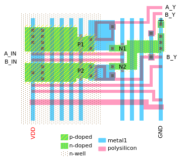
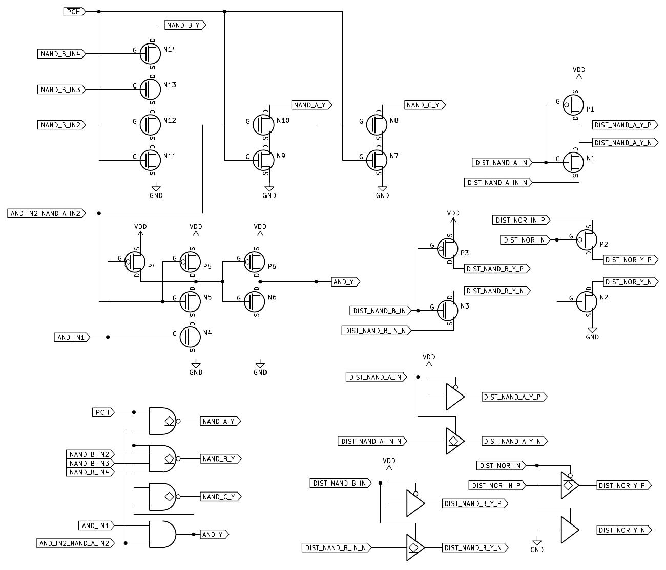
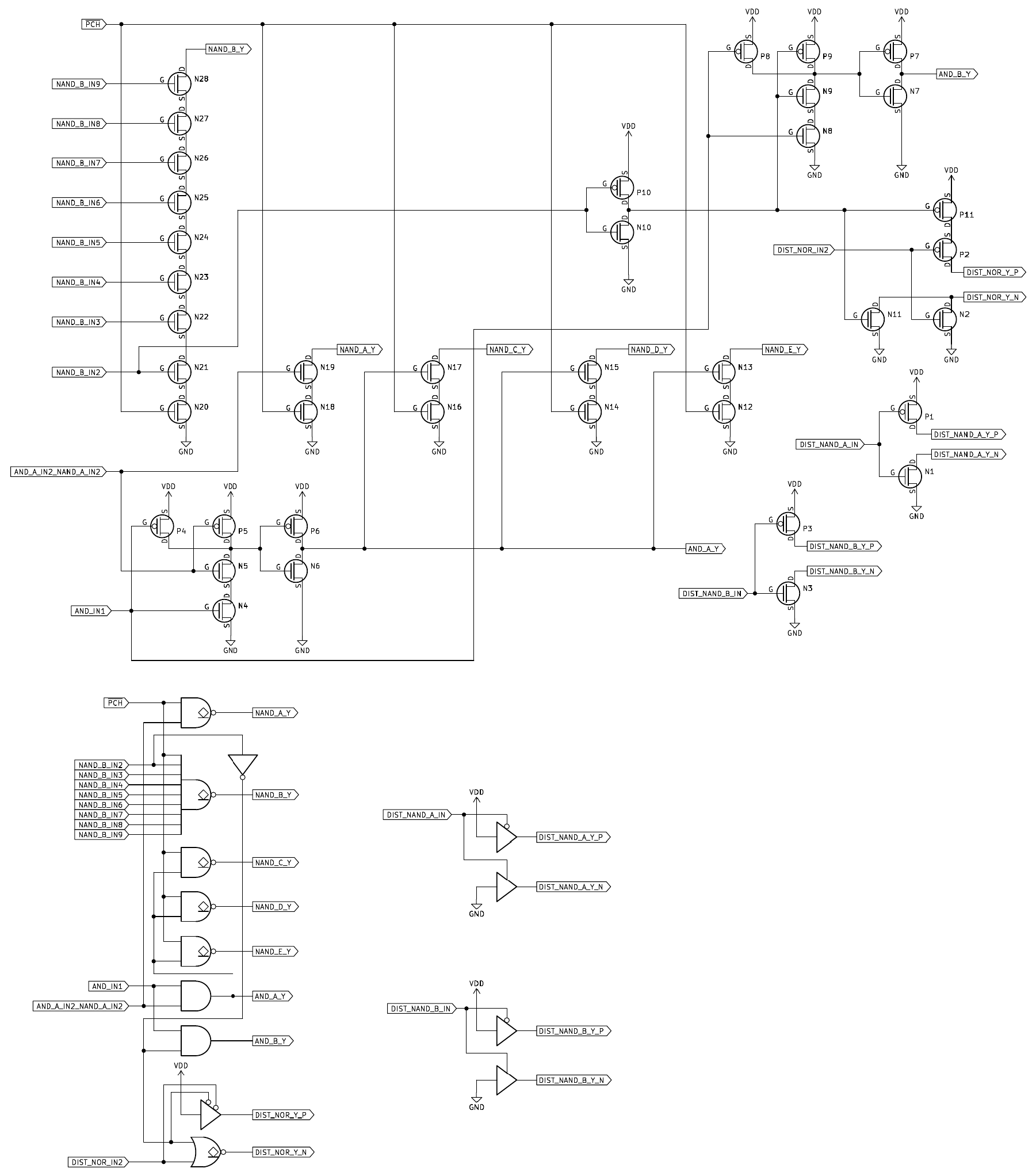
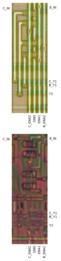
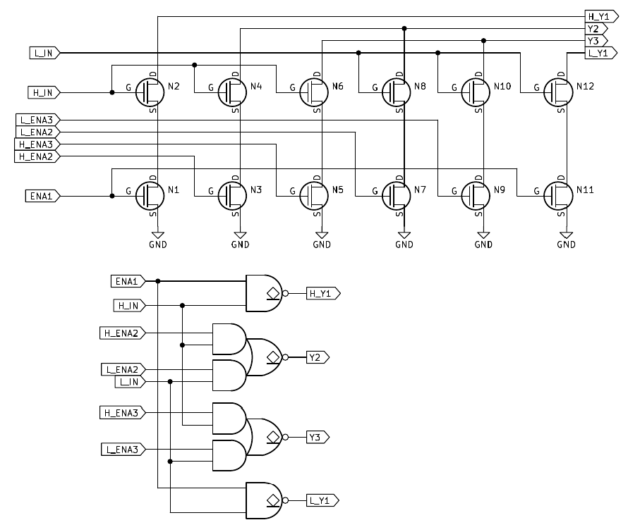
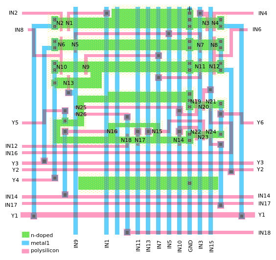
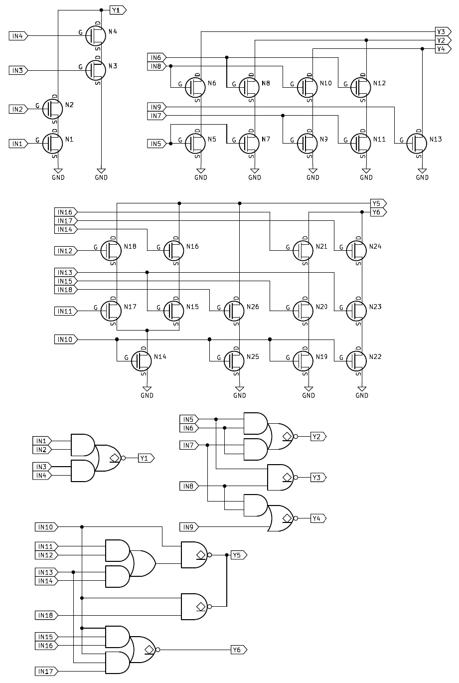
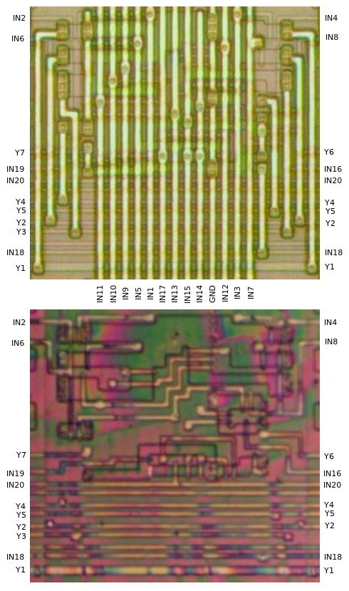
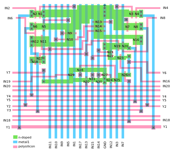
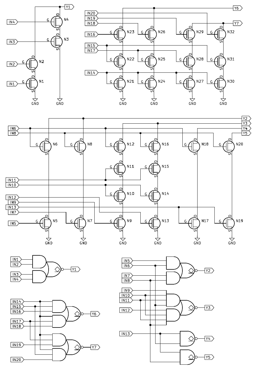
REG_BC_OUT
Output drivers for BC registers.
 |
| I/O | Description |
|---|
| B_IN |
Input to NAND gate B and AOI gate. |
| C_IN |
Input to NAND gate C and AOI gate. |
| ENA1 |
Input to both NAND gates. |
| B_ENA2, C_ENA2 |
Inputs to AOI gate. |
| B_Y1 |
Open-drain output. Outputs !(ENA1 && B_IN). |
| C_Y1 |
Open-drain output. Outputs !(ENA1 && C_IN). |
| Y2 |
Open-drain output. Outputs !((B_ENA2 && B_IN) || (C_ENA2 &&
C_IN)). |
|
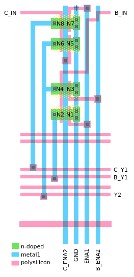
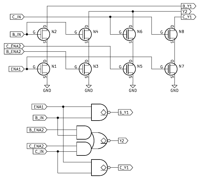
Instances:
REG_BC_OUT[0],
REG_BC_OUT[1],
REG_BC_OUT[2],
REG_BC_OUT[3],
REG_BC_OUT[4],
REG_BC_OUT[5],
REG_BC_OUT[6],
REG_BC_OUT[7]
(8 total)
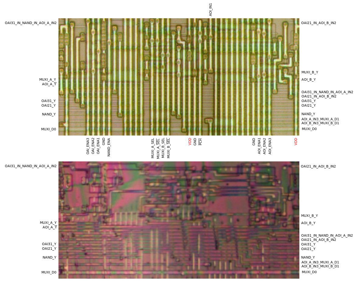
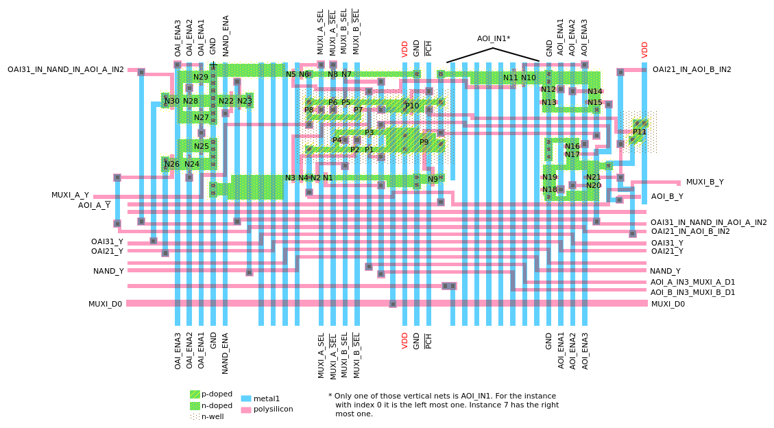
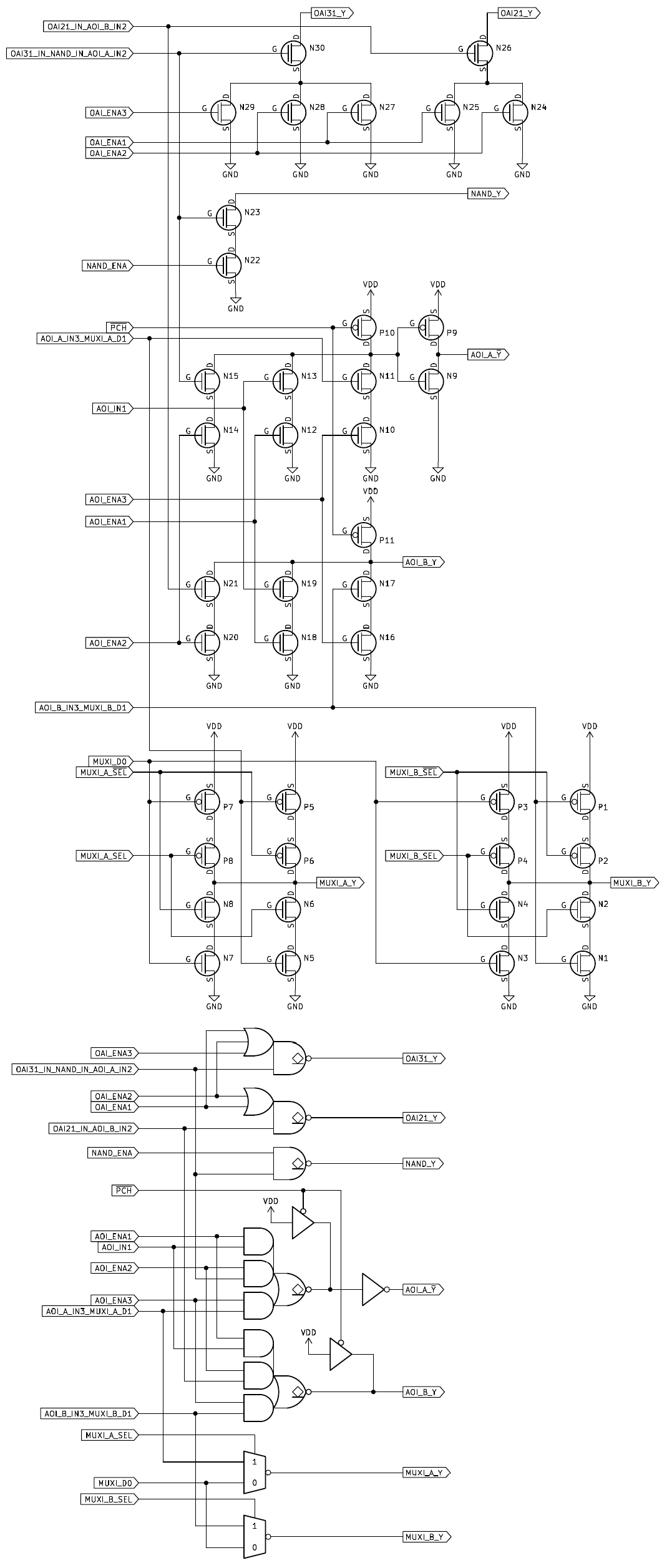
REG_BUS_PCH_A_BIT0123
Precharger and zero output for register busses bits 0-3.
There is one external connection always made on this cell (see orange line in the picture) that is required
to connect the two PCH inputs.
 |
| I/O | Description |
|---|
| PCH |
Active-low precharge input. If low, outputs A_Y, B_Y and C_Y get driven high for the
purpose of precharging their respective nets. There are two PCH
inputs to this cell, which are externally connected to each other (indicated by the orange line in the
picture). |
| C_ZERO |
If C_ZERO and PCH are both high, C_Y
outputs 0. |
| A_Y |
Open-source output. Outputs high if PCH is low. |
| B_Y |
Open-source output. Outputs high if PCH is low. |
| B_Y |
Outputs inverted B_Y. |
| C_Y |
Outputs low if C_ZERO and PCH are both high.
Outputs high if PCH is low. |
| C_Y |
Outputs inverted C_Y. |
|
Instances:
REG_BUS_PCH_A[0],
REG_BUS_PCH_A[1],
REG_BUS_PCH_A[2],
REG_BUS_PCH_A[3]
(4 total)
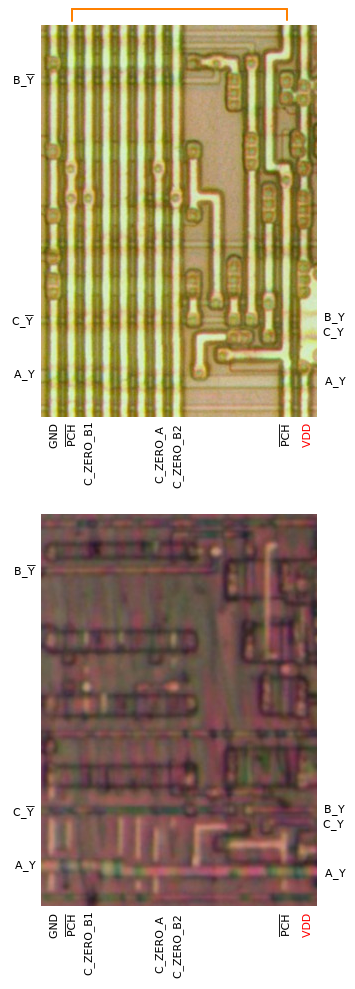
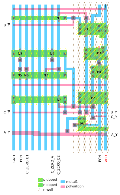
REG_BUS_PCH_A_BIT4
Precharger and zero output for register busses bit 4.
There is one external connection always made on this cell (see orange line in the picture) that is required
to connect the two PCH inputs.
 |
| I/O | Description |
|---|
| PCH |
Active-low precharge input. If low, outputs A_Y, B_Y and C_Y get driven high for the
purpose of precharging their respective nets. There are two PCH
inputs to this cell, which are externally connected to each other (indicated by the orange line in the
picture). |
| C_ZERO_A |
If C_ZERO_A and PCH are both high, C_Y
outputs 0. |
| C_ZERO_B1, C_ZERO_B2 |
If C_ZERO_B1, C_ZERO_B2 and PCH are high, C_Y
outputs 0. |
| A_Y |
Open-source output. Outputs high if PCH is low. |
| B_Y |
Open-source output. Outputs high if PCH is low. |
| B_Y |
Outputs inverted B_Y. |
| C_Y |
Outputs low if ((C_ZERO_A || (C_ZERO_B1 && C_ZERO_B2)) &&
PCH) is true. Outputs high if
PCH is low. |
| C_Y |
Outputs inverted C_Y. |
|
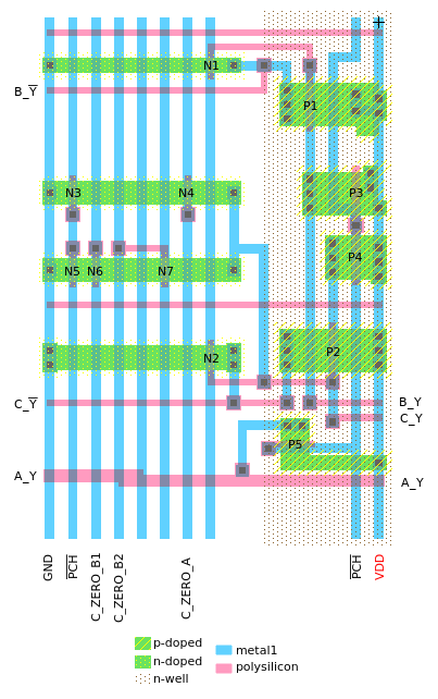
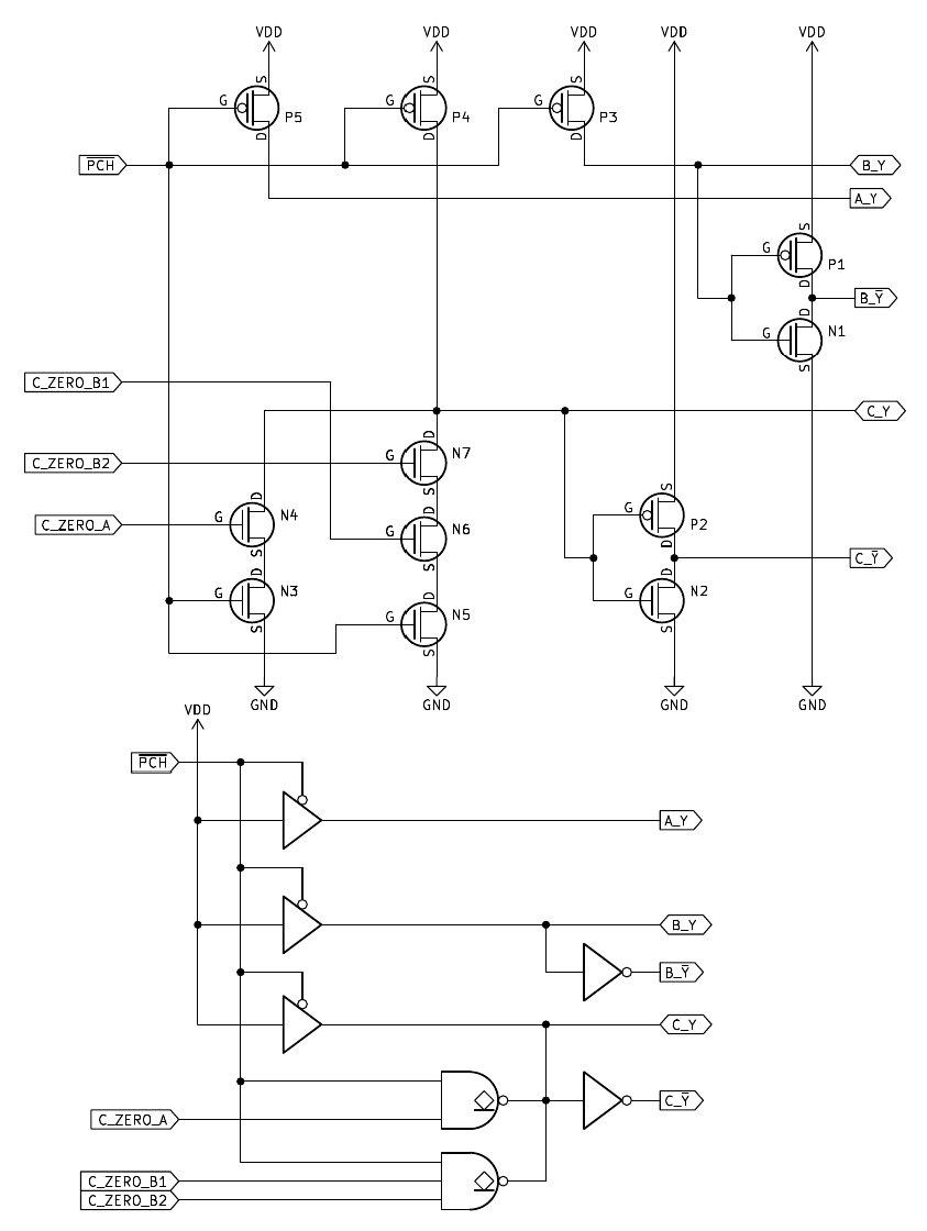
Instances:
REG_BUS_PCH_A[4]
(1 total)
REG_BUS_PCH_A_BIT5
Precharger and zero output for register busses bit 5.
There is one external connection always made on this cell (see orange line in the picture) that is required
to connect the two PCH inputs.
 |
| I/O | Description |
|---|
| PCH |
Active-low precharge input. If low, outputs A_Y, B_Y and C_Y get driven high for the
purpose of precharging their respective nets. There are two PCH
inputs to this cell, which are externally connected to each other (indicated by the orange line in the
picture). |
| C_ZERO_A |
If C_ZERO_A and PCH are both high, C_Y
outputs 0. |
| C_ZERO_B1, C_ZERO_B2 |
If C_ZERO_B1, C_ZERO_B2 and PCH are high, C_Y
outputs 0. |
| A_Y |
Open-source output. Outputs high if PCH is low. |
| B_Y |
Open-source output. Outputs high if PCH is low. |
| B_Y |
Outputs inverted B_Y. |
| C_Y |
Outputs low if ((C_ZERO_A || (C_ZERO_B1 && C_ZERO_B2)) &&
PCH) is true. Outputs high if
PCH is low. |
| C_Y |
Outputs inverted C_Y. |
|
Instances:
REG_BUS_PCH_A[5]
(1 total)
REG_BUS_PCH_A_BIT6
Precharger and zero output for register busses bit 6.
There is one external connection always made on this cell (see orange line in the picture) that is required
to connect the two PCH inputs.
 |
| I/O | Description |
|---|
| PCH |
Active-low precharge input. If low, outputs A_Y, B_Y and C_Y get driven high for the
purpose of precharging their respective nets. There are two PCH
inputs to this cell, which are externally connected to each other (indicated by the orange line in the
picture). |
| C_ZERO_A |
If C_ZERO_A and PCH are both high, C_Y
outputs 0. |
| C_ZERO_B1, C_ZERO_B2 |
If C_ZERO_B1, C_ZERO_B2 and PCH are high, C_Y
outputs 0. |
| A_Y |
Open-source output. Outputs high if PCH is low. |
| B_Y |
Open-source output. Outputs high if PCH is low. |
| B_Y |
Outputs inverted B_Y. |
| C_Y |
Outputs low if ((C_ZERO_A || (C_ZERO_B1 && C_ZERO_B2)) &&
PCH) is true. Outputs high if
PCH is low. |
| C_Y |
Outputs inverted C_Y. |
|
Instances:
REG_BUS_PCH_A[6]
(1 total)
REG_BUS_PCH_A_BIT7
Precharger and zero output for register busses bit 7.
There is one external connection always made on this cell (see orange line in the picture) that is required
to connect the two PCH inputs.
 |
| I/O | Description |
|---|
| PCH |
Active-low precharge input. If low, outputs A_Y, B_Y and C_Y get driven high for the
purpose of precharging their respective nets. There are two PCH
inputs to this cell, which are externally connected to each other (indicated by the orange line in the
picture). |
| C_ZERO_A |
If C_ZERO_A and PCH are both high, C_Y
outputs 0. |
| C_ZERO_B1, C_ZERO_B2 |
If C_ZERO_B1, C_ZERO_B2 and PCH are high, C_Y
outputs 0. |
| A_Y |
Open-source output. Outputs high if PCH is low. |
| B_Y |
Open-source output. Outputs high if PCH is low. |
| B_Y |
Outputs inverted B_Y. |
| C_Y |
Outputs low if ((C_ZERO_A || (C_ZERO_B1 && C_ZERO_B2)) &&
PCH) is true. Outputs high if
PCH is low. |
| C_Y |
Outputs inverted C_Y. |
|
Instances:
REG_BUS_PCH_A[7]
(1 total)
REG_BUS_PCH_B
Precharger for register busses.
 |
| I/O | Description |
|---|
| PCH |
Active-low precharge input. If low, outputs A_Y and B_Y get driven high for the purpose of
precharging their respective nets. |
| A_Y |
Open-source output. Outputs high if PCH is low. |
| B_Y |
Open-source output. Outputs high if PCH is low. |
|
Instances:
REG_BUS_PCH_B[0],
REG_BUS_PCH_B[1],
REG_BUS_PCH_B[2],
REG_BUS_PCH_B[3],
REG_BUS_PCH_B[4],
REG_BUS_PCH_B[5],
REG_BUS_PCH_B[6],
REG_BUS_PCH_B[7]
(8 total)
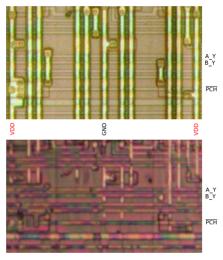
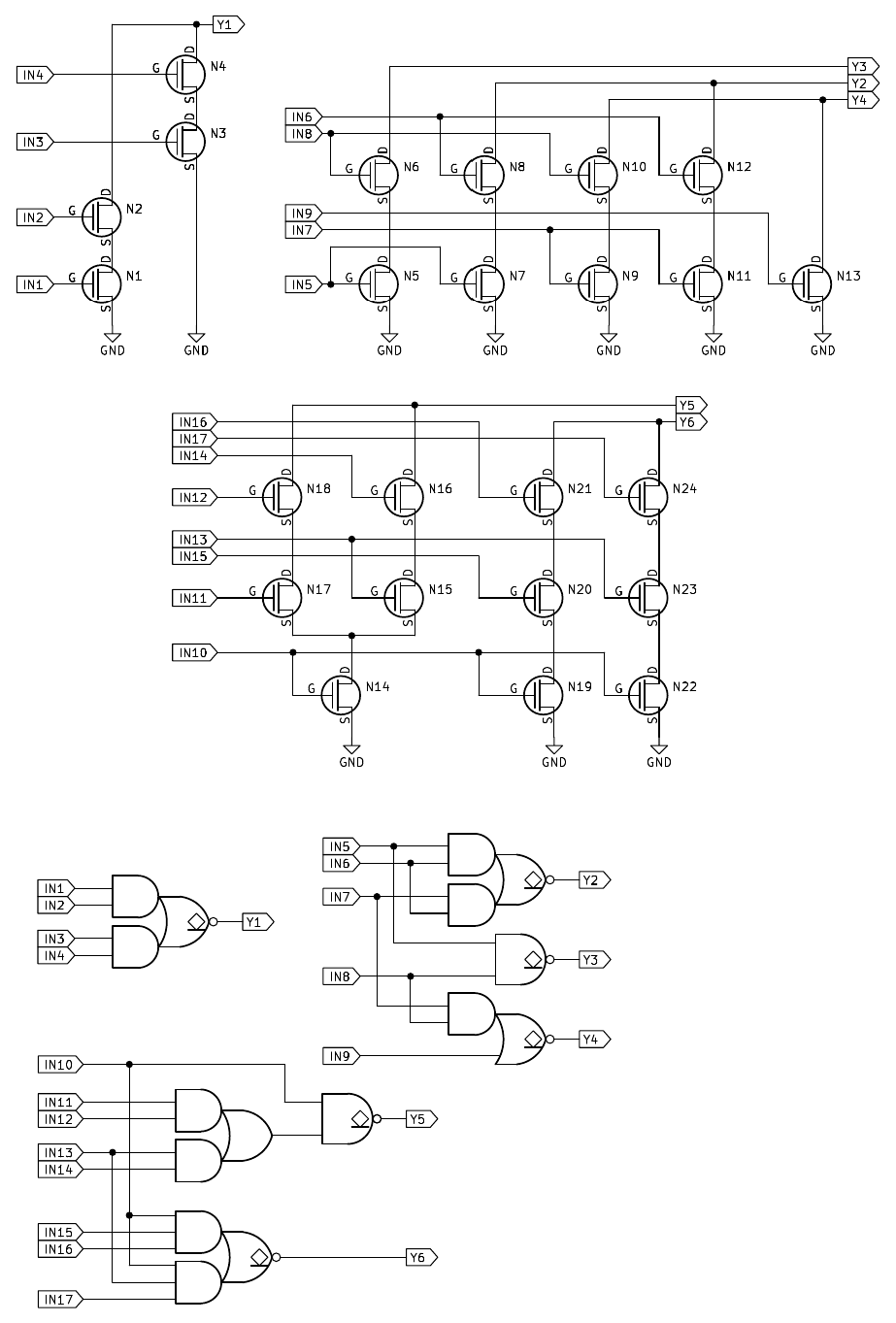
REG_DE_OUT
Output drivers for DE registers.
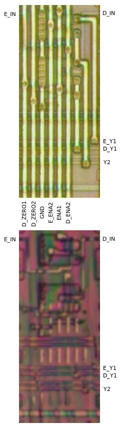 |
| I/O | Description |
|---|
| D_IN |
Input to NAND gate D and AOI gate. |
| E_IN |
Input to NAND gate E and AOI gate. |
| ENA1 |
Input to both NAND gates. |
| D_ENA2, E_ENA2 |
Inputs to AOI gate. |
| D_ZERO1, D_ZERO2 |
If D_ZERO1 or D_ZERO2 is high, D_Y1 outputs 0. |
| D_Y1 |
Open-drain output. Outputs (!(ENA1 && D_IN) && !D_ZERO1 &&
!D_ZERO2). |
| E_Y1 |
Open-drain output. Outputs !(ENA1 && E_IN). |
| Y2 |
Open-drain output. Outputs !((D_ENA2 && D_IN) || (E_ENA2 &&
E_IN)). |
|
Instances:
REG_DE_OUT[0],
REG_DE_OUT[1],
REG_DE_OUT[2],
REG_DE_OUT[3],
REG_DE_OUT[4],
REG_DE_OUT[5],
REG_DE_OUT[6],
REG_DE_OUT[7]
(8 total)
REG_HL_OUT
Output drivers for HL registers.
 |
| I/O | Description |
|---|
| |
TODO: Describe I/Os |
|
Instances:
REG_HL_OUT[0],
REG_HL_OUT[1],
REG_HL_OUT[2],
REG_HL_OUT[3],
REG_HL_OUT[4],
REG_HL_OUT[5],
REG_HL_OUT[6],
REG_HL_OUT[7]
(8 total)
REG_PC_OUT_BIT012
Output drivers for PC register bits 0-2.
 |
| I/O | Description |
|---|
| |
TODO: Describe I/Os |
|
Instances:
REG_PC_OUT[0],
REG_PC_OUT[1],
REG_PC_OUT[2]
(3 total)
REG_PC_OUT_BIT345
Output drivers for PC register bits 3-5.
 |
| I/O | Description |
|---|
| |
TODO: Describe I/Os |
|
Instances:
REG_PC_OUT[3],
REG_PC_OUT[4],
REG_PC_OUT[5]
(3 total)
REG_PC_OUT_BIT67
Output drivers for PC register bits 6 and 7.
 |
| I/O | Description |
|---|
| |
TODO: Describe I/Os |
|
Instances:
REG_PC_OUT[6],
REG_PC_OUT[7]
(2 total)
REG_SP_OUT
Output drivers for SP registers.
 |
| I/O | Description |
|---|
| |
TODO: Describe I/Os |
|
Instances:
REG_SP_OUT[0],
REG_SP_OUT[1],
REG_SP_OUT[2],
REG_SP_OUT[3],
REG_SP_OUT[4],
REG_SP_OUT[5],
REG_SP_OUT[6],
REG_SP_OUT[7]
(8 total)
REG_WZ_OUT
Output drivers for WZ registers.
| I/O | Description |
|---|
| |
TODO: Describe I/Os |
Instances:
REG_WZ_OUT[0],
REG_WZ_OUT[1],
REG_WZ_OUT[2],
REG_WZ_OUT[3],
REG_WZ_OUT[4],
REG_WZ_OUT[5],
REG_WZ_OUT[6],
REG_WZ_OUT[7]
(8 total)
Storage elements
SRLATCH_R_N
SR-latch with active-high set input and active-low reset input. Reset takes precedence when both inputs
are asserted.
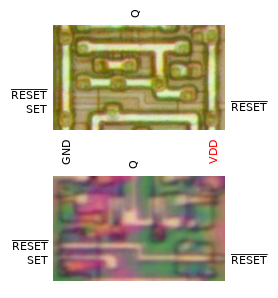 |
| I/O | Description |
|---|
| SET |
Set input. When high, latch is set to 1. Has no effect when
RESET is low at the same time. |
| RESET |
Inverted reset input. When low, latch is set to 0. |
| Q |
Data output. |
|
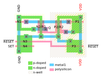
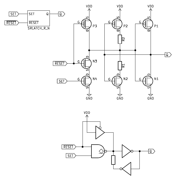
Instances:
ZJJE,
ZKOG,
ZLOZ,
ZOJZ,
ZRSY,
ZUMN
(6 total)
SRLATCH_R_N_ALT
SR-latch with active-high set input and active-low reset input. Reset takes precedence when both inputs
are asserted.
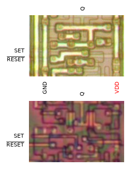 |
| I/O | Description |
|---|
| SET |
Set input. When high, latch is set to 1. Has no effect when
RESET is low at the same time. |
| RESET |
Inverted reset input. When low, latch is set to 0. |
| Q |
Data output. |
|

Instances:
YNKW
(1 total)
DLATCH_EE_Q_N
Gated data latch with externally inverted enable inputs and no non-inverted output.
There are two enable inputs to this cell. They need to be inverted towards each other.
 |
| I/O | Description |
|---|
| D |
Data input. |
| ENA |
Active-high enable input. When high, the value at D transparently propagates through the latch. As soon
as ENA goes low, the output of the latch gets held at the level it had in that moment until ENA goes
high again. |
| ENA |
Active-low enable input. Must always be the inverse of ENA. |
| Q |
Inverted data output. |
|
Instances:
YODP
(1 total)
DLATCH_EE_IRQ
Gated data latch with externally inverted enable inputs and additional dynamically controlled inverted output.
There are two enable inputs to this cell. They need to be inverted towards each other.
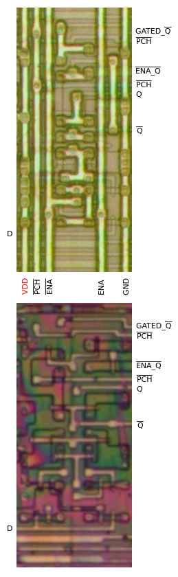 |
| I/O | Description |
|---|
| D |
Data input. |
| ENA |
Active-high enable input. When high, the value at D transparently propagates through the latch. As soon
as ENA goes low, the output of the latch gets held at the level it had in that moment until ENA goes
high again. |
| ENA |
Active-low enable input. Must always be the inverse of ENA. |
| Q |
Data output. |
| Q |
Inverted data output. |
| GATED_Q |
Dynamically gated inverted data output. Outputs Q when
ENA_Q is low, otherwise outputs low. Needs to be precharged
regularly by pulling PCH low and making
ENA_Q hi-Z at the same time. |
| ENA_Q |
Active-low enable input for dynamically gated GATED_Q output.
Must be undriven (hi-Z) when PCH is enabled/low. |
| PCH |
Active-low precharge input. If low, GATED_Q gets driven
low. Must be disabled/high when ENA_Q is enabled/low. |
|
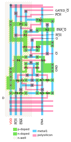
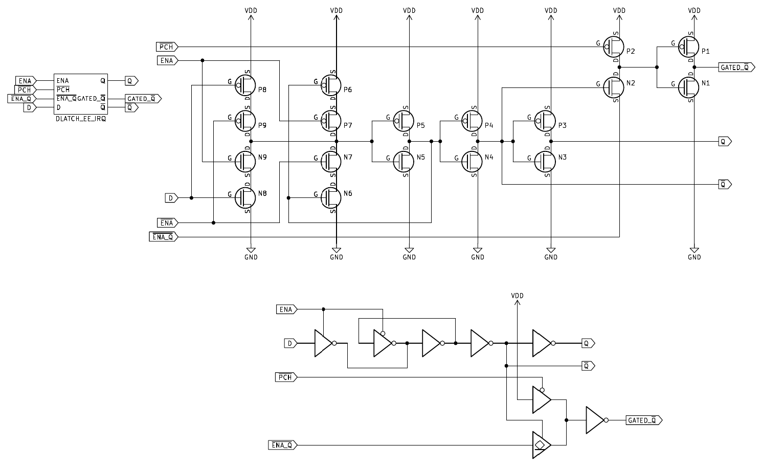
Instances:
IRQ_LATCH[0],
IRQ_LATCH[1],
IRQ_LATCH[2],
IRQ_LATCH[3],
IRQ_LATCH[4],
IRQ_LATCH[5],
IRQ_LATCH[6],
IRQ_LATCH[7]
(8 total)
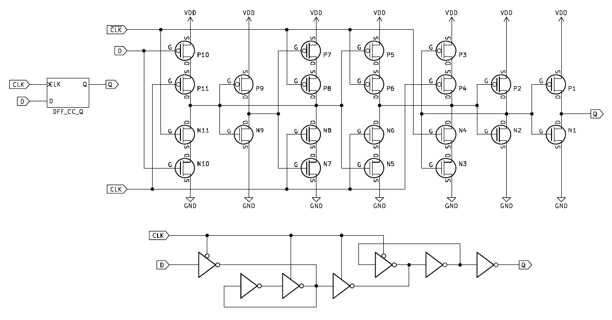
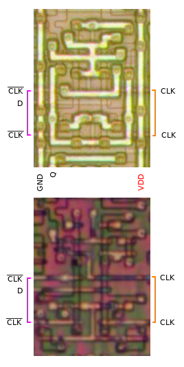
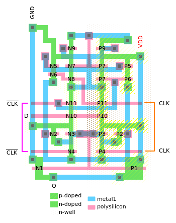
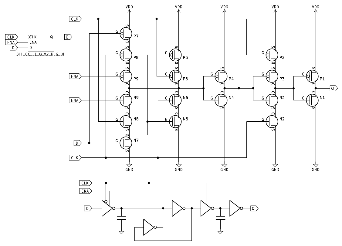
DFF_CC_Q
Single-edge-triggered data flip-flop with complementary clock inputs and no inverted output.
There are two clock inputs to this cell. They need to be inverted towards each other. The flip-flop triggers
on a positive edge of CLK and a negative edge of CLK.
There are two external connections always made on this cell (see pink and orange lines in the picture).
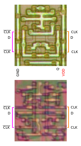 |
| I/O | Description |
|---|
| D |
Data input. Gets stored in the flip-flop on positive edge of CLK and a simultanious negative edge of
CLK. |
| CLK |
Positive clock input. On a positive edge the data input D gets stored in the flip-flop. There needs
to be a negative edge on the CLK input at the same time.
There are two CLK inputs to this cell, which are externally connected to each other (indicated by the
orange line in the picture). |
| CLK |
Negative clock input. On a negative edge the data input D gets stored in the flip-flop. There needs
to be a positive edge on the CLK input at the same time. There are two
CLK inputs to this cell, which are externally connected
to each other (indicated by the pink line in the picture). |
| Q |
Data output. |
|
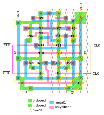
Instances:
XAYM,
XDQF,
XIRF,
XOGS,
YDXA,
YOII,
YSBT,
ZACW,
ZAZA,
ZIVV,
ZKAI,
ZKDU,
ZORP,
ZRBY
(14 total)
DFF_CC_Q_ALT
Single-edge-triggered data flip-flop with complementary clock inputs and no inverted output.
There are two clock inputs to this cell. They need to be inverted towards each other. The flip-flop triggers
on a positive edge of CLK and a negative edge of CLK.
There are two external connections always made on this cell (see pink and orange lines in the picture).
 |
| I/O | Description |
|---|
| D |
Data input. Gets stored in the flip-flop on positive edge of CLK and a simultanious negative edge of
CLK. |
| CLK |
Positive clock input. On a positive edge the data input D gets stored in the flip-flop. There needs
to be a negative edge on the CLK input at the same time.
There are two CLK inputs to this cell, which are externally connected to each other (indicated by the
orange line in the picture). |
| CLK |
Negative clock input. On a negative edge the data input D gets stored in the flip-flop. There needs
to be a positive edge on the CLK input at the same time. There are two
CLK inputs to this cell, which are externally connected
to each other (indicated by the pink line in the picture). |
| Q |
Data output. |
|
Instances:
XUFU
(1 total)
DFF_CC_EE_Q_X1_REG_BIT
Semi-dynamic data flip-flop with complementary clock inputs, externally inverted enable inputs, level-sensitive
D-gating, and no inverted output.
 |
| I/O | Description |
|---|
| D |
Data input. Gets stored in the flip-flop when CLK is low and ENA is high. However, the new data
is only visible at the output Q after a positive edge on CLK. |
| CLK |
Positive clock input. Edge sensitive for presenting stored data at output; level sensitive for taking new data
from input into storage. When CLK is low and ENA is high, the data input D gets stored in
the flip-flop. After a positive edge on CLK, the newly stored data is visible at the output Q.
CLK must not be held low for an extended amount of time, otherwise the stored data will decay. |
| CLK |
Negative clock input. Must always be the inverse of CLK. |
| ENA |
Active-high enable input. Input D gets stored in the flip-flop when ENA is high and CLK
is low. |
| ENA |
Active-low enable input. Must always be the inverse of ENA. |
| Q |
Data output. |
|
Instances:
REG_B[0],
REG_B[1],
REG_B[2],
REG_B[3],
REG_B[4],
REG_B[5],
REG_B[6],
REG_B[7],
REG_C[0],
REG_C[1],
REG_C[2],
REG_C[3],
REG_C[4],
REG_C[5],
REG_C[6],
REG_C[7],
REG_D[0],
REG_D[1],
REG_D[2],
REG_D[3],
REG_D[4],
REG_D[5],
REG_D[6],
REG_D[7],
REG_E[0],
REG_E[1],
REG_E[2],
REG_E[3],
REG_E[4],
REG_E[5],
REG_E[6],
REG_E[7],
REG_H[0],
REG_H[1],
REG_H[2],
REG_H[3],
REG_H[4],
REG_H[5],
REG_H[6],
REG_H[7],
REG_L[0],
REG_L[1],
REG_L[2],
REG_L[3],
REG_L[4],
REG_L[5],
REG_L[6],
REG_L[7]
(48 total)
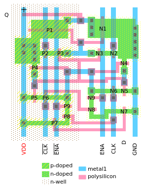
DFF_CC_EE_Q_X2_REG_BIT
Semi-dynamic data flip-flop with complementary clock inputs, externally inverted enable inputs, level-sensitive
D-gating, 2× drive strength, and no inverted output.
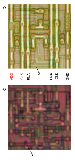 |
| I/O | Description |
|---|
| D |
Data input. Gets stored in the flip-flop when CLK is low and ENA is high. However, the new data
is only visible at the output Q after a positive edge on CLK. |
| CLK |
Positive clock input. Edge sensitive for presenting stored data at output; level sensitive for taking new data
from input into storage. When CLK is low and ENA is high, the data input D gets stored in
the flip-flop. After a positive edge on CLK, the newly stored data is visible at the output Q.
CLK must not be held low for an extended amount of time, otherwise the stored data will decay. |
| CLK |
Negative clock input. Must always be the inverse of CLK. |
| ENA |
Active-high enable input. Input D gets stored in the flip-flop when ENA is high and CLK
is low. |
| ENA |
Active-low enable input. Must always be the inverse of ENA. |
| Q |
Data output. |
|
Instances:
REG_A[0],
REG_A[1],
REG_A[2],
REG_A[3],
REG_A[4],
REG_A[5],
REG_A[6],
REG_A[7],
REG_IR[0],
REG_IR[1],
REG_IR[2],
REG_IR[3],
REG_IR[4],
REG_IR[5],
REG_IR[6],
REG_IR[7]
(16 total)
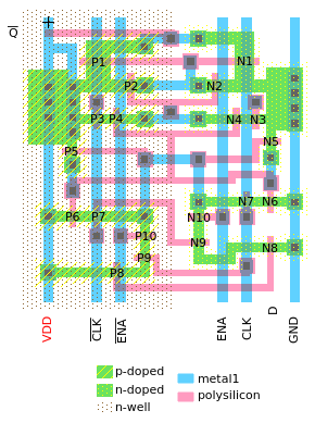
DFF_CC_EE_PCH_D_REG_SP_BIT
Semi-dynamic data flip-flop with complementary clock inputs, externally inverted enable inputs, level-sensitive
D-gating, and prechargable D input.
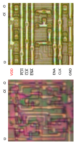 |
| I/O | Description |
|---|
| D |
Data input. Gets stored in the flip-flop when CLK is low and ENA is high. However, the new data
is only visible at the outputs Q and Q after a positive
edge on CLK. Outputs high if PCH is low. |
| PCH |
Active-low precharge input. If low, D gets driven high for the purpose of precharging the net
connected to the input. |
| CLK |
Positive clock input. Edge sensitive for presenting stored data at output; level sensitive for taking new data
from input into storage. When CLK is low and ENA is high, the data input D gets stored in
the flip-flop. After a positive edge on CLK, the newly stored data is visible at the outputs Q and
Q. CLK must not be held low for an extended amount of
time, otherwise the stored data will decay. |
| CLK |
Negative clock input. Must always be the inverse of CLK. |
| ENA |
Active-high enable input. Input D gets stored in the flip-flop when ENA is high and CLK
is low. |
| ENA |
Active-low enable input. Must always be the inverse of ENA. |
| Q |
Data output. |
| Q |
Inverted data output. |
|
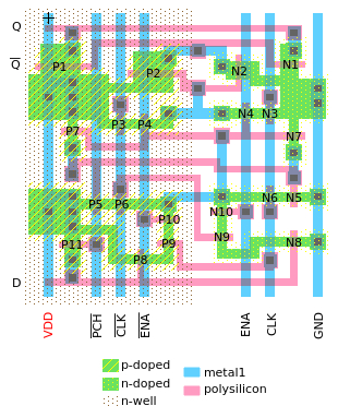
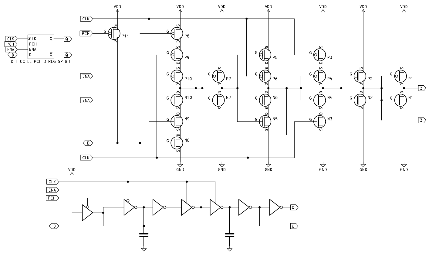
Instances:
REG_SPH[0],
REG_SPH[1],
REG_SPH[2],
REG_SPH[3],
REG_SPH[4],
REG_SPH[5],
REG_SPH[6],
REG_SPH[7],
REG_SPL[0],
REG_SPL[1],
REG_SPL[2],
REG_SPL[3],
REG_SPL[4],
REG_SPL[5],
REG_SPL[6],
REG_SPL[7]
(16 total)
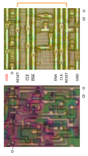
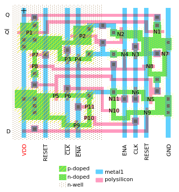
DFF_CC_EE_Q_N_REG_WZ_BIT
Semi-dynamic data flip-flop with complementary clock inputs, externally inverted enable inputs, level-sensitive
D-gating, and no non-inverted output.
 |
| I/O | Description |
|---|
| D |
Data input. Gets stored in the flip-flop when CLK is low and ENA is high. However, the new data
is only visible at the output Q after a positive
edge on CLK. |
| CLK |
Positive clock input. Edge sensitive for presenting stored data at output; level sensitive for taking new data
from input into storage. When CLK is low and ENA is high, the data input D gets stored in
the flip-flop. After a positive edge on CLK, the newly stored data is visible at the output
Q. CLK must not be held low for an extended amount of
time, otherwise the stored data will decay. |
| CLK |
Negative clock input. Must always be the inverse of CLK. |
| ENA |
Active-high enable input. Input D gets stored in the flip-flop when ENA is high and CLK
is low. |
| ENA |
Active-low enable input. Must always be the inverse of ENA. |
| Q |
Inverted data output. |
|
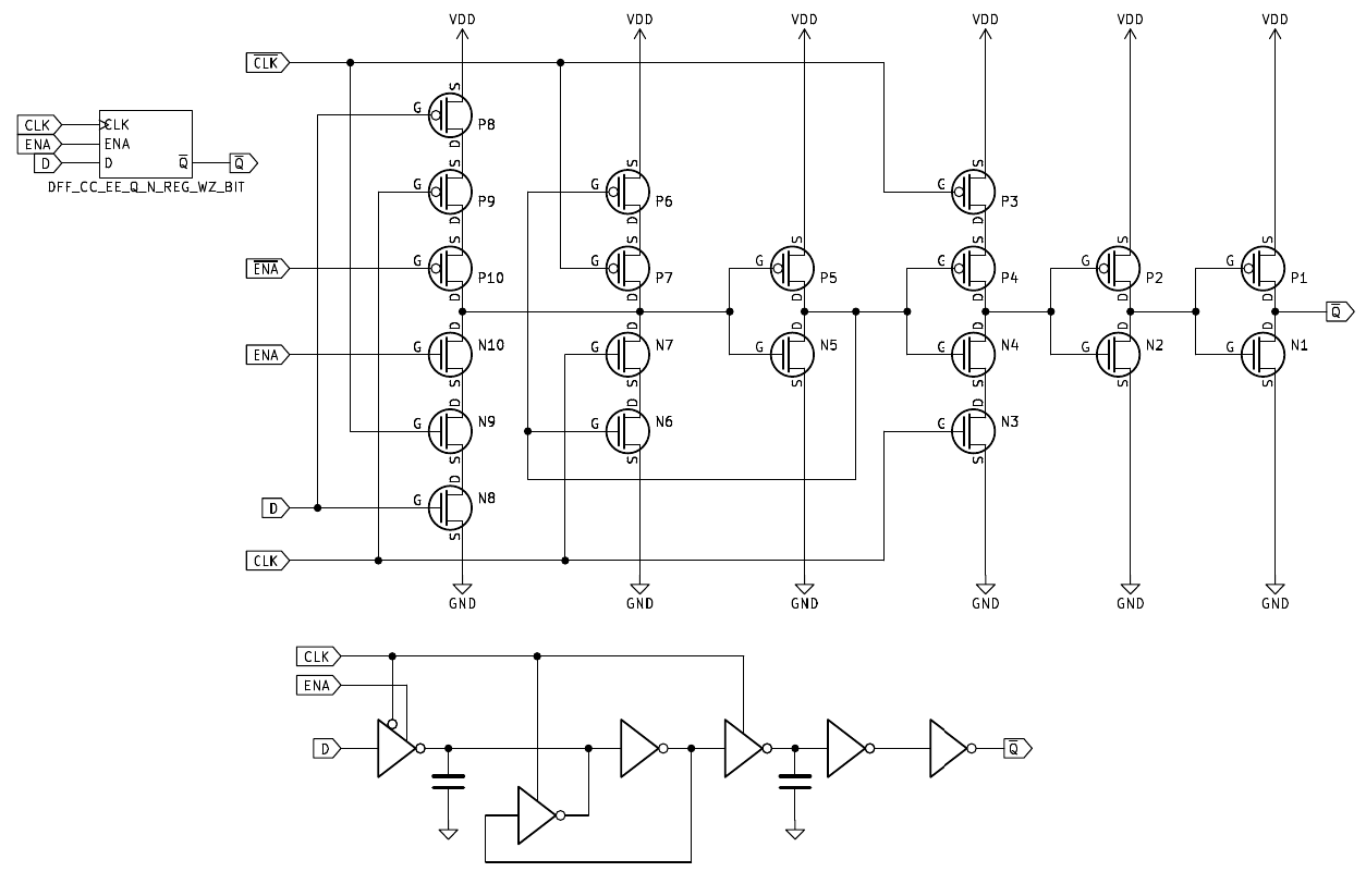
Instances:
REG_W[0],
REG_W[1],
REG_W[2],
REG_W[3],
REG_W[4],
REG_W[5],
REG_W[6],
REG_W[7],
REG_Z[0],
REG_Z[1],
REG_Z[2],
REG_Z[3],
REG_Z[4],
REG_Z[5],
REG_Z[6],
REG_Z[7]
(16 total)
DFFR_CC_EE_REG_IE_BIT
Semi-dynamic data flip-flop with complementary clock inputs, externally inverted enable inputs, level-sensitive
D-gating, and active-high reset gated by the clock level.
There is one external connection always made on this cell (see orange line in the picture) that is required
to connect the two RESET inputs.
 |
| I/O | Description |
|---|
| D |
Data input. Gets stored in the flip-flop when CLK and RESET are both low and ENA is high.
However, the new data is only visible at the outputs Q and
Q after a positive edge on CLK. |
| CLK |
Positive clock input. Edge sensitive for presenting stored data at output; level sensitive for taking new data
from input into storage. When CLK and RESET are both low and ENA is high, the data input D
gets stored in the flip-flop. After a positive edge on CLK, the newly stored data is visible at the outputs
Q and Q. CLK must not be held low for an extended
amount of time, otherwise the stored data will decay. |
| CLK |
Negative clock input. Must always be the inverse of CLK. |
| ENA |
Active-high enable input. Input D gets stored in the flip-flop when ENA is high and CLK
and RESET are both low. |
| ENA |
Active-low enable input. Must always be the inverse of ENA. |
| RESET |
Active-high reset input. Data inside the flip-flop gets reset to 0 when RESET and CLK are both high.
Has no effect while CLK is low. There are two RESET inputs to this cell, which are externally connected
to each other (indicated by the orange line in the picture). |
| Q |
Data output. |
| Q |
Inverted data output. |
|
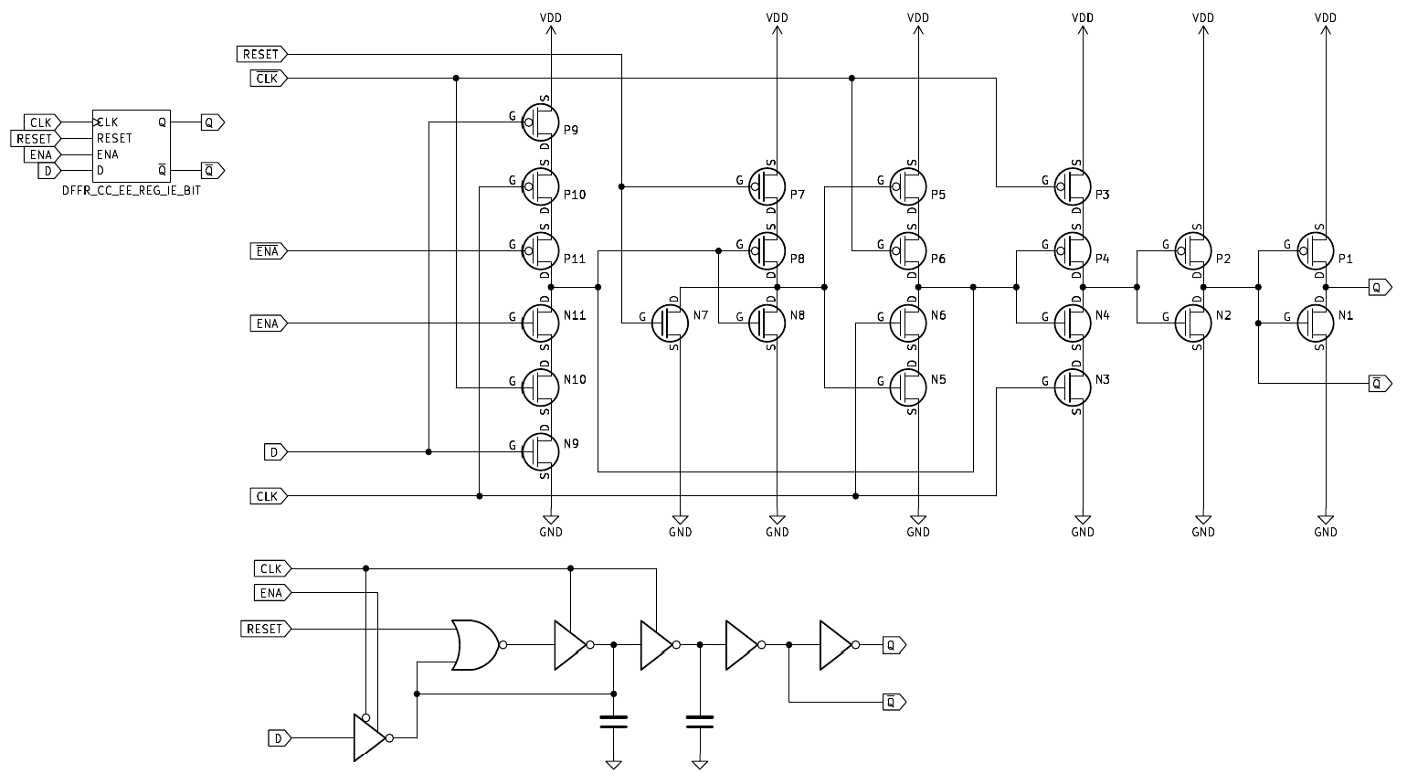
Instances:
REG_IE[0],
REG_IE[1],
REG_IE[2],
REG_IE[3],
REG_IE[4],
REG_IE[5],
REG_IE[6],
REG_IE[7]
(8 total)
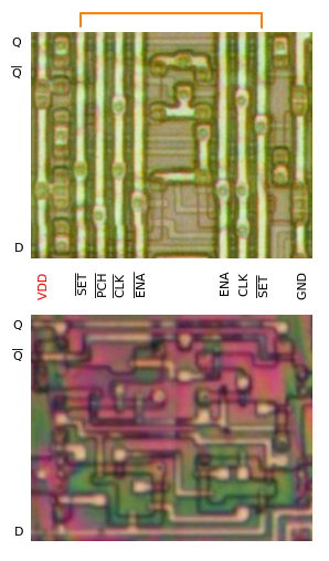
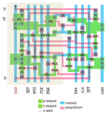
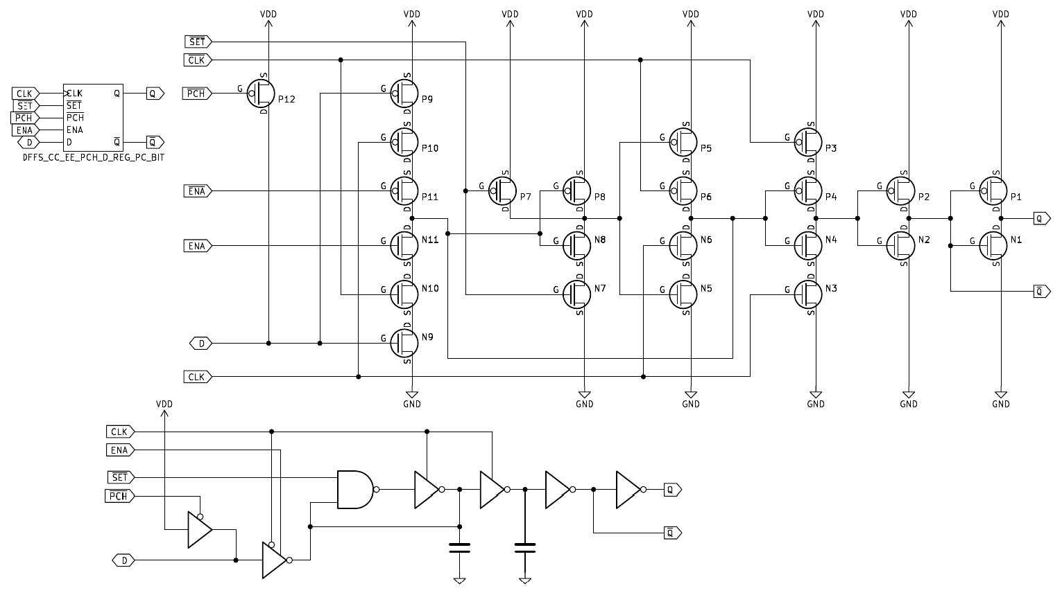
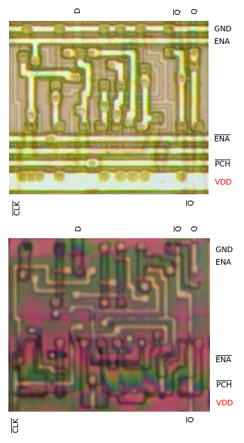
DFFS_CC_EE_PCH_D_REG_PC_BIT
Semi-dynamic data flip-flop with complementary clock inputs, externally inverted enable inputs, level-sensitive
D-gating, prechargable D input, and active-low set gated by the clock level.
There is one external connection always made on this cell (see orange line in the picture) that is required
to connect the two SET inputs.
 |
| I/O | Description |
|---|
| D |
Data input. Gets stored in the flip-flop when CLK is low and ENA and
SET are both high.
However, the new data is only visible at the outputs Q and
Q after a positive edge on CLK. |
| PCH |
Active-low precharge input. If low, D gets driven high for the purpose of precharging the net
connected to the input. |
| CLK |
Positive clock input. Edge sensitive for presenting stored data at output; level sensitive for taking new data
from input into storage. When CLK is low and ENA and
SET are both high, the data input D gets stored in the
flip-flop. After a positive edge on CLK, the newly stored data is visible at the outputs Q and
Q. CLK must not be held low for an extended amount of
time, otherwise the stored data will decay. |
| CLK |
Negative clock input. Must always be the inverse of CLK. |
| ENA |
Active-high enable input. Input D gets stored in the flip-flop when ENA and
SET are both high and CLK is low. |
| ENA |
Active-low enable input. Must always be the inverse of ENA. |
| SET |
Active-low set input. Data inside the flip-flop gets set to 1 when
SET is low and CLK is high. Has no effect while CLK
is low. There are two SET inputs to this cell, which are
externally connected to each other (indicated by the orange line in the picture). |
| Q |
Data output. |
| Q |
Inverted data output. |
|
Instances:
REG_PCH[0],
REG_PCH[1],
REG_PCH[2],
REG_PCH[3],
REG_PCH[4],
REG_PCH[5],
REG_PCH[6],
REG_PCH[7],
REG_PCL[0],
REG_PCL[1],
REG_PCL[2],
REG_PCL[3],
REG_PCL[4],
REG_PCL[5],
REG_PCL[6],
REG_PCL[7]
(16 total)
DFFN_EE_PCH_D_ALU_FLAG
Semi-dynamic data flip-flop with externally inverted enable inputs, level-sensitive D-gating, and prechargable
D input.
 |
| I/O | Description |
|---|
| D |
Data input. Gets stored in the flip-flop when CLK and
ENA are both high. However, the new data is only visible at the outputs Q and
Q after a negative edge on
CLK. Outputs high if
PCH is low. |
| PCH |
Active-low precharge input. If low, D gets driven high for the purpose of precharging the net
connected to the input. |
| CLK |
Clock input. Edge sensitive for presenting stored data at output; level sensitive for taking new data from input
into storage. When CLK and ENA are both high, the data
input D gets stored in the flip-flop. After a negative edge on
CLK, the newly stored data is visible at the outputs Q
and Q. CLK
must not be held high for an extended amount of time, otherwise the stored data will decay. |
| ENA |
Active-high enable input. Input D gets stored in the flip-flop when ENA and
CLK are both high. |
| ENA |
Active-low enable input. Must always be the inverse of ENA. |
| Q |
Data output. |
| Q |
Inverted data output. |
|
Instances:
FLAG_C,
FLAG_H,
FLAG_N,
FLAG_Z
(4 total)
DFFN_EE_Q_ALU_SIGN
Semi-dynamic data flip-flop with externally inverted enable inputs, level-sensitive D-gating, and no inverted
output.
 |
| I/O | Description |
|---|
| D |
Data input. Gets stored in the flip-flop when CLK and
ENA are both high. However, the new data is only visible at the output Q after a negative edge on
CLK. |
| CLK |
Clock input. Edge sensitive for presenting stored data at output; level sensitive for taking new data from input
into storage. When CLK and ENA are both high, the data
input D gets stored in the flip-flop. After a negative edge on
CLK, the newly stored data is visible at the output Q.
CLK must not be held high for an extended amount of time,
otherwise the stored data will decay. |
| ENA |
Active-high enable input. Input D gets stored in the flip-flop when ENA and
CLK are both high. |
| ENA |
Active-low enable input. Must always be the inverse of ENA. |
| Q |
Data output. |
|
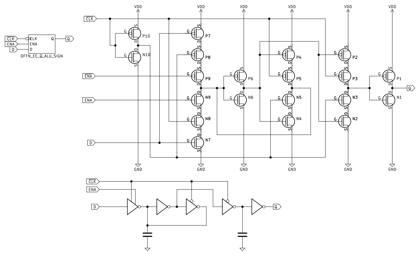
Instances:
ALU_DFF
(1 total)
DFFRE_CC_Q
Semi-dynamic data flip-flop with complementary clock inputs, level-sensitive D-gating, active-high reset
gated by the clock level, and no inverted output.
 |
| I/O | Description |
|---|
| D |
Data input. Gets stored in the flip-flop when CLK and RESET are both low and ENA is high.
However, the new data is only visible at the output Q after a positive edge on CLK. |
| CLK |
Positive clock input. Edge sensitive for presenting stored data at output; level sensitive for taking new data
from input into storage. When CLK and RESET are both low and ENA is high, the data input D
gets stored in the flip-flop. After a positive edge on CLK, the newly stored data is visible at the output
Q. CLK must not be held low for an extended amount of time, otherwise the stored data will decay. |
| CLK |
Negative clock input. Must always be the inverse of CLK. |
| ENA |
Active-high enable input. Input D gets stored in the flip-flop when ENA is high and CLK
and RESET are both low. |
| RESET |
Active-high reset input. Data inside the flip-flop gets reset to 0 when RESET and CLK are both high.
Has no effect while CLK is low. |
| Q |
Data output. |
|
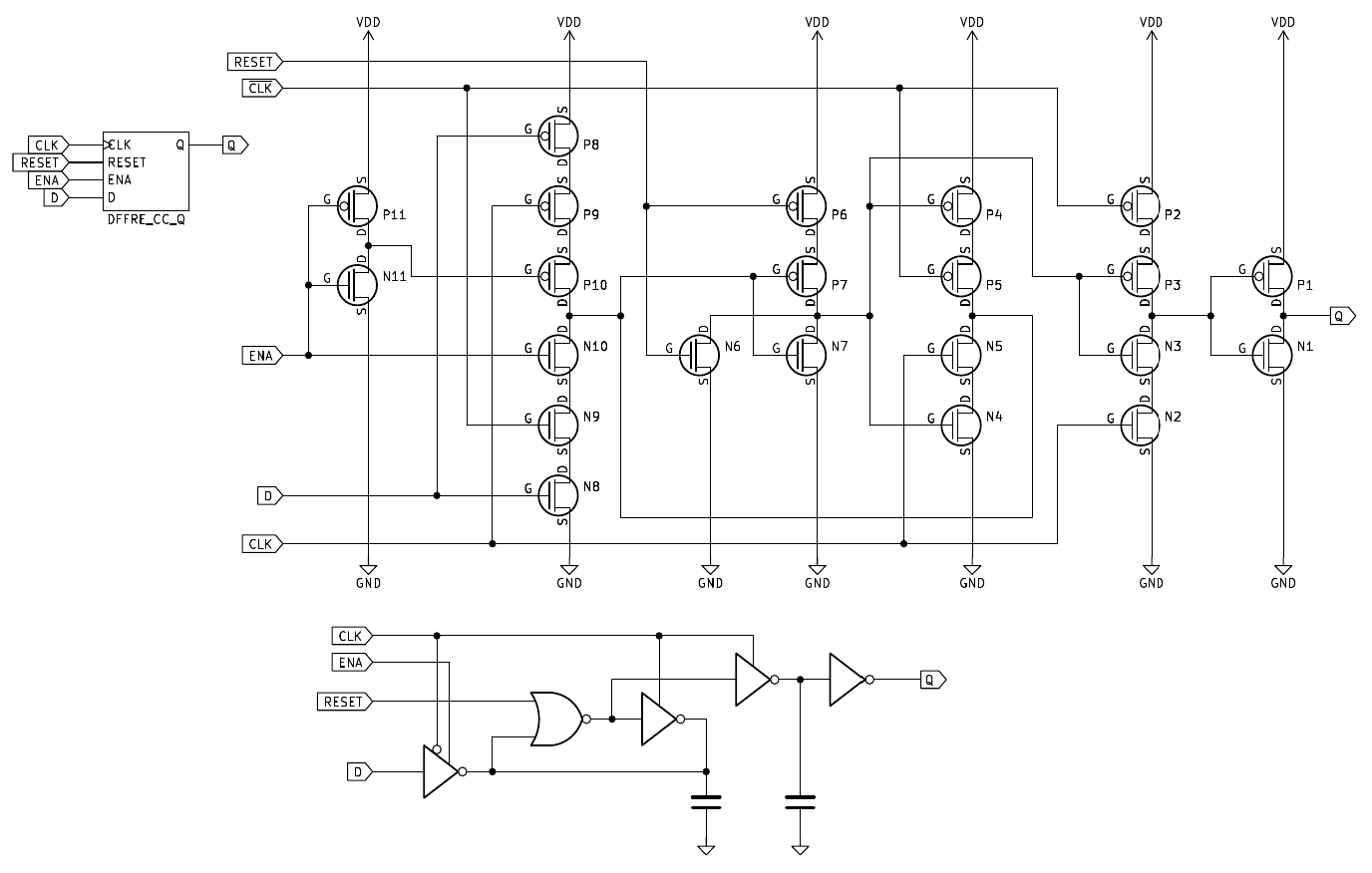
Instances:
XURG
(1 total)