DMG-CPU SM83 Core Connections
This is a list of all connections to/from the SM83 CPU core as seen in the Gameboy DMG-CPU-B die shot. The wire and cell names are taken from our schematics of the DMG-CPU B.
For a deeper understanding of the CPU, you should have a look at the reverse engineering efforts of ogamespec and Gekkio. Or you can play with the visual6502 port of the CPU.
Please report any errors I made here.
SM83 "Pinout"
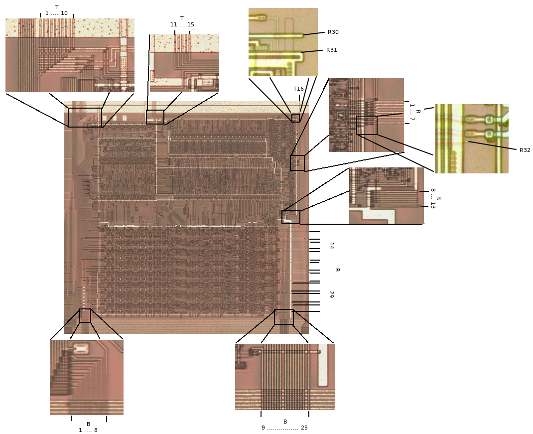
SM83 Connections
| I/O | Port Name | Wire Name | Description | |
|---|---|---|---|---|
| T1 | O | M1 | CTL_FETCH | Machine cycle one (M1) synchronization signal. High during the instruction fetch cycle (M1).Ticks: : T1 : T2 : T3 : T4 : CLK4MiHz: ‾‾|__|‾‾|__|‾‾|__|‾‾|__ M1: __|‾‾‾‾‾‾‾‾‾‾‾‾‾‾‾‾‾‾‾‾| |
| T2 | I | EXEC_PHASE | EXEC_PHASE | A gated 1 MiHz clock, which goes low the moment the CPU outputs the new address at the beginning of a
memory cycle. It is low while the address is valid on the cartridge port and high during the short time when the
address high byte on the cartridge port is usually zeroed. The rising edge of this clock updates the DFF that stores the effective IME (Interrupt Master Enable) flag. The CPU can stop this clock by driving HALT (T11) low, in which case it stays permanently high. This is the inverse of EXEC_PHASE (T3).
Ticks:       : T1  : T2  : T3  : T4  :
CLK4MiHz:     ‾‾|__|‾‾|__|‾‾|__|‾‾|__
EXEC_PHASE:   ‾‾|____________________|
|
| T3 | I | EXEC_PHASE | EXEC_PHASE | A gated 1 MiHz clock, which goes high the moment the CPU outputs the new address at the beginning of a
memory cycle. It is high while the address is valid on the cartridge port and low during the short time when the
address high byte on the cartridge port is usually zeroed. Most control signals generated from the dynamic NMOS decoders are valid while this clock is high, and are precharged while it is low. This clock is also responsible for precharging other components while it is low: Internal and external data bus, dynamic NMOS logic of ALU, ALU operand buses, and the input bus of the increment/decrement unit (IDU). The CPU can stop this clock by driving HALT (T11) low, in which case it stays permanently low. This is the inverse of EXEC_PHASE (T2). Ticks: : T1 : T2 : T3 : T4 : CLK4MiHz: ‾‾|__|‾‾|__|‾‾|__|‾‾|__ EXEC_PHASE: __|‾‾‾‾‾‾‾‾‾‾‾‾‾‾‾‾‾‾‾‾| |
| T4 | I | DATA_PHASE | DATA_PHASE | A gated 1 MiHz clock, which is identical to the 1 MiHz PHI clock signal on the cartridge port. While this clock is high, IRQ_LATCH[0..7] are enabled. The CPU can stop this clock by driving HALT (T11) low, in which case it stays permanently high. This is the inverse of DATA_PHASE (T5).
Ticks:       : T1  : T2  : T3  : T4  :
CLK4MiHz:     ‾‾|__|‾‾|__|‾‾|__|‾‾|__
DATA_PHASE:   ‾‾‾‾‾‾‾‾‾‾‾|___________|
|
| T5 | I | DATA_PHASE | DATA_PHASE | A gated 1 MiHz clock, which is the inverse of the 1 MiHz PHI clock signal on the cartridge port. The few control signals generated by the dynamic NMOS decoders that are not timed by EXEC_PHASE (T3), are valid while DATA_PHASE is high. Those signals are write enable control signals for registers and flags. It makes sense that those are only asserted during the data phase where the value on the data bus is valid. While DATA_PHASE is low, those signals are precharged. DATA_PHASE also precharges the following: Dynamic NMOS logic that drives new values for writing registers, NMOS chains in increment/decrement unit (IDU). It also controls some latches in the interrupt logic part of the sequencer, and it gives shape to the RD (R1) signal. The CPU can stop this clock by driving HALT (T11) low, in which case it stays permanently low. This is the inverse of DATA_PHASE (T4). Ticks: : T1 : T2 : T3 : T4 : CLK4MiHz: ‾‾|__|‾‾|__|‾‾|__|‾‾|__ DATA_PHASE: ___________|‾‾‾‾‾‾‾‾‾‾‾| |
| T6 | I | WRITE_PHASE | WRITE_PHASE | A gated 1 MiHz clock, which is low during the fourth quarter of each memory cycle. The CPU can stop this clock by driving HALT (T11) low, in which case it stays permanently high. This is the inverse of WRITE_PHASE (T7).
Ticks:       : T1  : T2  : T3  : T4  :
CLK4MiHz:     ‾‾|__|‾‾|__|‾‾|__|‾‾|__
WRITE_PHASE:  ‾‾‾‾‾‾‾‾‾‾‾‾‾‾‾‾‾|_____|
|
| T7 | I | WRITE_PHASE | WRITE_PHASE | A gated 1 MiHz clock, which is high during the fourth quarter of each memory cycle. Registers and flags are written during the high phase of this clock when their respective write enable signals are also asserted. When this clock is low, some dynamic NMOS logic responsible for interrupt priority decoding is precharged. The CPU can stop this clock by driving HALT (T11) low, in which case it stays permanently low. This is the inverse of WRITE_PHASE (T6). Ticks: : T1 : T2 : T3 : T4 : CLK4MiHz: ‾‾|__|‾‾|__|‾‾|__|‾‾|__ WRITE_PHASE: _________________|‾‾‾‾‾| |
| T8 | I | PCH_PHASE | PCH_PHASE | A gated 1 MiHz clock, which goes high when WRITE_PHASE (T7) goes high, and low when
EXEC_PHASE (T2) and CLK (T10) go low. During its low phase, this clock is responsible for precharging the dynamic NMOS logic in the ALU that produces the new values for the ALU flags, and also for precharging the dynamic NMOS logic that produces the new PC and SP. The CPU can stop this clock by driving HALT (T11) low, in which case it stays permanently low. This is the only clock that goes into the CPU that has no inverse counterpart.
Ticks:       : T1  : T2  : T3  : T4  :
CLK4MiHz:     ‾‾|__|‾‾|__|‾‾|__|‾‾|__
PCH_PHASE:    ‾‾|______________|‾‾‾‾‾
|
| T9 | I | CLK | CLK | A gated 1 MiHz clock, which goes high the moment the CPU outputs the new address at the beginning of a
memory cycle. It is high while the address is valid on the cartridge port and low during the short time when the
address high byte on the cartridge port is usually zeroed. This is the inverse of CLK (T10). CLK (T9) and CLK (T10) are the only clock inputs that are ticking during HALT mode. When the oscillator is stopped, this clock stays permanently low.
Ticks:       : T1  : T2  : T3  : T4  :
CLK4MiHz:     ‾‾|__|‾‾|__|‾‾|__|‾‾|__
CLK:          __|‾‾‾‾‾‾‾‾‾‾‾‾‾‾‾‾‾‾‾‾|
|
| T10 | I | CLK | CLK | A gated 1 MiHz clock, which goes low the moment the CPU outputs the new address at the beginning of a
memory cycle. It is low while the address is valid on the cartridge port and high during the short time when the
address high byte on the cartridge port is usually zeroed. The rising edge of this clock is only used by the sequencer logic, for advancing the machine cycle and for some interrupt processing. This is the inverse of CLK (T9). CLK (T9) and CLK (T10) are the only clock inputs that are ticking during HALT mode. When the oscillator is stopped, this clock stays permanently high. Ticks: : T1 : T2 : T3 : T4 : CLK4MiHz: ‾‾|__|‾‾|__|‾‾|__|‾‾|__ CLK: ‾‾|____________________| |
| T11 | O | HALT | HALT | CPU can drive this low to disable most of the clocks fed to itself. CLK
(T9) and CLK (T10) are the only clocks that are not turned off when this signal gets driven low. When PWRON_RESET (T13) is asserted during power-on-reset, HALT is initialized to low state, so most CPU clocks are disabled. The CPU must NOT switch this signal to high immediately after reset, otherwise SYS_RESET (T12) (generated by AFER) and the synchronous peripheral resets (RESET2, APU_RESETn, PPU_RESETn, ...) will never be deasserted. The CPU must wait until CLK_READY (T15) (generated by TABA) gets high. This happens when the DIV register is half run through, which takes about 32 milliseconds. The CPU pulls HALT (T11) high when CLK_READY (T15) is high and SYS_RESET (T12) is low, but delayed by one CLK rising edge. I assume this mechanism is there to assure the crystal oscillator is stabilized. The same mechanism is used when the system wakes up from STOP mode. When the crystal oscillator gets disabled by driving STOP (T14) low, the DIV register gets reset to zero, so it will take the same ~32 ms. When the CPU executes a HALT instruction and none of the enabled interrupts are pending, then the CPU will pull HALT (T11) low to disable most of its clocks. When waking up from HALT mode (due to an interrupt), the CPU will pull HALT (T11) high on the next CLK rising edge, which re-enables all the other clocks. Changes to the HALT output are always synchonized to the rising edge of CLK (T10). TODO: Test if an externally clocked SERIAL interrupt can bypass the 32 ms period when resuming from STOP mode. |
| T12 | I | SYS_RESET | SYS_RESET | Active-high system reset input. Supposed to be synchronized to the rising edge of CLK (T10). The program counter (PC) and the interrupt enable register (IE) are both reset to 0 by this reset. Also the sequencer state is reset to perform an initial instruction fetch. Nothing else is being reset in the CPU. Other registers will have random values, including the instruction register. This means the CPU can execute a random instruction in parallel to the initial fetch cycle. However, it can't execute any jumps or memory accesses (except the instruction fetch), because no instruction encodes these actions on M cycle 7 (which is the initial state). |
| T13 | I | PWRON_RESET | PWRON_RESET | Active-high power-on reset input. Fed directly from
RESET input pad. This reset is necessary on power-on to initialize the state of the HALT (T11) output to low and the STOP (T14) output to high, so that the crystal oscillator gets enabled. It resets nothing else. SYS_RESET (T12) is used to bring the CPU into a valid initial state once CLK/CLK (T10/T9) are ticking. |
| T14 | O | STOP | STOP | When CPU drives this low, the crystal oscillator
gets disabled to save power. This happens during STOP mode. HALT (T11)
will also be low during STOP mode. A change to STOP from high to low will always be synchonized to the rising edge of CLK (T10). A change from low to high happens immediately when WAKE (B25) is high. |
| T15 | I | CLK_READY | CLK_READY | On power-on reset or when waking up from STOP mode, this signal gets high after about 32 milliseconds to signal to the CPU that the clocks are stable. The CPU will acknowledge this signal by pulling HALT (T11) high, which in turn deasserts CLK_READY. See description of HALT (T11) for more details. |
| T16 | I | NMI | NMI | Directly connected to an input pad at the top of the die, which is not bonded. This is the non-maskable interrupt of the CPU. |
| R1 | O | RD | RD | Active-high memory read signal from CPU. In contrast to the read signal on the cartridge connector, the CPU its read
signal is only asserted when the CPU actually reads data. It is synchronous to the DATA_PHASE (T5) clock. When the CPU is
reading from its internal IE register on address 0xFFFF, the read signal is also asserted. Although the read signal is only asserted during T3 and T4, data on the bus is sampled for much longer (see diagram below). The sampling doesn't happen on an edge, it happens while EXEC_PHASE (T3) is high. If at any time during this sampling period a data bit on the bus is low, then it will be read as low, even if it flips back to high later. So basically, the read operation works like an AND operation over time. When there is the value 0xFC on the data bus at T2 and the value 0x3F at T4, then the CPU will read the value 0x3C, because 0xFC ∧ 0x3F = 0x3C. The data bus is always precharged to 0xFF during the first half-cycle of T1. Ticks: : T1 : T2 : T3 : T4 : CLK4MiHz: ‾‾|__|‾‾|__|‾‾|__|‾‾|__ RD: ___________|‾‾‾‾‾‾‾‾‾‾‾| D[0..7]: ‾‾|XXXXXXXXXXXXXXXXXXXX| |
| R2 | O | WR | WR | Active-high memory write signal from CPU. The write signal is synchronous to the EXEC_PHASE (T3) clock. When the CPU
is writing to its internal IE register on address 0xFFFF, the write signal is also asserted. Although the write signal is already asserted at the falling edge of T1, the data is only valid while DATA_PHASE (T5) is high (which is during T3 and T4). The data bus is always precharged to 0xFF during the first half-cycle of T1. At any other time, the data is only actively driven low. This means the same AND rule applies like during a read operation: If by accident, someone is driving a low bit onto the data bus (for example at T2), then this bit will stay low until the precharging at the beginning of the next memory cycle happens. Ticks: : T1 : T2 : T3 : T4 : CLK4MiHz: ‾‾|__|‾‾|__|‾‾|__|‾‾|__ WR: __|‾‾‾‾‾‾‾‾‾‾‾‾‾‾‾‾‾‾‾‾| D[0..7]: ‾‾‾‾‾‾‾‾‾‾‾|XXXXXXXXXXX| |
| R3 | I | OE | OE | Active-low output enable. When high, then D[0..7] (B1-B8) and A[0..15] (B9-B24) are disabled and not
actively driven by the CPU, and RD (R1) is disabled by being driven low. WR (R2) is not affected. This is only used when test mode T1 is enabled. |
| R4 | I | INTERNAL_ACCESS | INTERNAL_ACCESS | When high, then the MREQ (R7) output is inhibited and stays low. The circuit outside the CPU drives this input high when address bus is 0xFEXX or 0xFFXX. |
| R5 | I | SHADOW_ACCESS | SHADOW_ACCESS | When high while SHADOW_OVERRIDE (R6) is low, then the MREQ (R7) output is inhibited and stays low. The circuit outside the CPU drives this input high when address bus is 0x00XX and boot ROM is still visible. |
| R6 | I | SHADOW_OVERRIDE | SHADOW_OVERRIDE | When high, this disables the function of the SHADOW_ACCESS (R5) input. This is only used when test mode T2 is enabled. |
| R7 | O | MREQ | MREQ | Active-high external memory request. High during external memory cycles (read or write). This causes one of the
chip select signals
(CS,
MCS,
A15) to be asserted in the right moment. Low if no memory cycle is going on,
otherwise the chip select would be asserted even if RD (R1) and WR (R2) are low. During write cycles, this signal
is also needed for driving the internal data bus onto the external I/O pins. During read cycles, this signal is also
needed for latching the external I/O pins and driving the latched data onto the chip internal data bus. When
INTERNAL_ACCESS (R4) or SHADOW_ACCESS (R5) is high, the CPU keeps this signal low, allowing internal components
(HRAM, OAM, boot ROM, FFxx registers) to drive the data bus. To be precise, MREQ is asserted during a memory cycle when this is true: ¬INTERNAL_ACCESS ∧ (¬SHADOW_ACCESS ∨ SHADOW_OVERRIDE) Ticks: : T1 : T2 : T3 : T4 : CLK4MiHz: ‾‾|__|‾‾|__|‾‾|__|‾‾|__ MREQ: __|‾‾‾‾‾‾‾‾‾‾‾‾‾‾‾‾‾‾‾‾| |
| R8 | - | - | VDD | Not connected. Internally connected to VDD. |
| R9 | - | - | VDD | Not connected. Internally connected to VDD. |
| R10 | - | - | GND | Not connected. Internally connected to GND. |
| R11 | - | - | GND | Not connected. Internally connected to GND. |
| R12 | - | - | GND | Not connected. Internally connected to GND. |
| R13 | O | FFXX | FFXX | Not connected. High when A[15..8] (B9-B16) are high. |
| R14 | O | INTA[0] | INTA[0] | Active-high. Acknowledges IRQ0 (V-Blank).
Ticks: : T1 : T2 : T3 : T4 : CLK4MiHz: ‾‾|__|‾‾|__|‾‾|__|‾‾|__ INTA[0]: _________________|‾‾‾‾‾| |
| R15 | I | INT[0] | INT[0] | Active-high. Triggers IRQ0 (V-Blank). |
| R16 | O | INTA[1] | INTA[1] | Active-high. Acknowledges IRQ1 (Status).
Ticks: : T1 : T2 : T3 : T4 : CLK4MiHz: ‾‾|__|‾‾|__|‾‾|__|‾‾|__ INTA[1]: _________________|‾‾‾‾‾| |
| R17 | I | INT[1] | INT[1] | Active-high. Triggers IRQ1 (Status). |
| R18 | O | INTA[2] | INTA[2] | Active-high. Acknowledges IRQ2 (Timer).
Ticks: : T1 : T2 : T3 : T4 : CLK4MiHz: ‾‾|__|‾‾|__|‾‾|__|‾‾|__ INTA[2]: _________________|‾‾‾‾‾| |
| R19 | I | INT[2] | INT[2] | Active-high. Triggers IRQ2 (Timer). |
| R20 | O | INTA[3] | INTA[3] | Active-high. Acknowledges IRQ3 (Serial).
Ticks: : T1 : T2 : T3 : T4 : CLK4MiHz: ‾‾|__|‾‾|__|‾‾|__|‾‾|__ INTA[3]: _________________|‾‾‾‾‾| |
| R21 | I | INT[3] | INT[3] | Active-high. Triggers IRQ3 (Serial). |
| R22 | O | INTA[4] | INTA[4] | Active-high. Acknowledges IRQ4 (Joypad).
Ticks: : T1 : T2 : T3 : T4 : CLK4MiHz: ‾‾|__|‾‾|__|‾‾|__|‾‾|__ INTA[4]: _________________|‾‾‾‾‾| |
| R23 | I | INT[4] | INT[4] | Active-high. Triggers IRQ4 (Joypad). |
| R24 | O | INTA[5] | INTA[5] | Active-high. Acknowledges IRQ5. Not connected.
Ticks: : T1 : T2 : T3 : T4 : CLK4MiHz: ‾‾|__|‾‾|__|‾‾|__|‾‾|__ INTA[5]: _________________|‾‾‾‾‾| |
| R25 | I | INT[5] | INT[5] | Active-high. Triggers IRQ5. Hardwired to GND. |
| R26 | O | INTA[6] | INTA[6] | Active-high. Acknowledges IRQ6. Not connected.
Ticks: : T1 : T2 : T3 : T4 : CLK4MiHz: ‾‾|__|‾‾|__|‾‾|__|‾‾|__ INTA[6]: _________________|‾‾‾‾‾| |
| R27 | I | INT[6] | INT[6] | Active-high. Triggers IRQ6. Hardwired to GND. |
| R28 | O | INTA[7] | INTA[7] | Active-high. Acknowledges IRQ7. Not connected.
Ticks: : T1 : T2 : T3 : T4 : CLK4MiHz: ‾‾|__|‾‾|__|‾‾|__|‾‾|__ INTA[7]: _________________|‾‾‾‾‾| |
| R29 | I | INT[7] | INT[7] | Active-high. Triggers IRQ7. Hardwired to GND. |
| R30 | O | PREFIX_CB | CTL_OP_CB_PREFIX | Not connected. High when the currently executed opcode is 0xCB.
Ticks: : T1 : T2 : T3 : T4 : CLK4MiHz: ‾‾|__|‾‾|__|‾‾|__|‾‾|__ PREFIX_CB: __|‾‾‾‾‾‾‾‾‾‾‾‾‾‾‾‾‾‾‾‾| |
| R31 | I | TEST_FREEZE | TEST_FREEZE | Hardwired to GND. I assume this was used for testing the CPU. When pulled high, the current M cycle in the sequencer is set to 7, and the TABLE_CB and IN_INTR inputs of the first instruction decoder stage are temporarily overriden to be true, which is an invalid state. In this state the CPU would just do nothing until TEST_FREEZE is released again. |
| R32 | O | INT_ENTRY | INT_ENTRY | Not connected. High while an interrupt entry sequence is executed. Changes state on rising edges of CLK (T10). |
| B1 | I/O | D[0] | D[0] | Data bus D[0]. |
| B2 | I/O | D[1] | D[1] | Data bus D[1]. |
| B3 | I/O | D[2] | D[2] | Data bus D[2]. |
| B4 | I/O | D[3] | D[3] | Data bus D[3]. |
| B5 | I/O | D[4] | D[4] | Data bus D[4]. |
| B6 | I/O | D[5] | D[5] | Data bus D[5]. |
| B7 | I/O | D[6] | D[6] | Data bus D[6]. |
| B8 | I/O | D[7] | D[7] | Data bus D[7]. |
| B9 | O | A[15] | A[15] | Address bus A[15]. |
| B10 | O | A[14] | A[14] | Address bus A[14]. |
| B11 | O | A[13] | A[13] | Address bus A[13]. |
| B12 | O | A[12] | A[12] | Address bus A[12]. |
| B13 | O | A[11] | A[11] | Address bus A[11]. |
| B14 | O | A[10] | A[10] | Address bus A[10]. |
| B15 | O | A[9] | A[9] | Address bus A[9]. |
| B16 | O | A[8] | A[8] | Address bus A[8]. |
| B17 | O | A[7] | A[7] | Address bus A[7]. |
| B18 | O | A[6] | A[6] | Address bus A[6]. |
| B19 | O | A[5] | A[5] | Address bus A[5]. |
| B20 | O | A[4] | A[4] | Address bus A[4]. |
| B21 | O | A[3] | A[3] | Address bus A[3]. |
| B22 | O | A[2] | A[2] | Address bus A[2]. |
| B23 | O | A[1] | A[1] | Address bus A[1]. |
| B24 | O | A[0] | A[0] | Address bus A[0]. |
| B25 | I | WAKE | WAKE | Wakes CPU from STOP mode. Rising this signal immediately causes the CPU to pull STOP (T14) high, which enables the crystal oscillator. Has no effect when STOP is already high. |